Home > Press > Imec reports record efficiencies for large-area epitaxial thin-film silicon solar cells
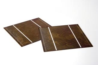 |
| Imec epitaxial thin-film silicon solar cell on low-quality substrate with screen printed metal lines achieving efficiencies of up to 14.7%. |
Abstract:
Imec has realized large-area (70cm2) epitaxial solar cells with efficiencies of up to 16.3% on high-quality substrates. And efficiencies of up to 14.7% were achieved on large-area low-quality substrates, showing the potential of thin-film epitaxial solar cells for industrial manufacturing. The results were achieved within imec's silicon solar cell industrial affiliation program (IIAP) that explores and develops advanced process technologies aiming a sharp reduction in silicon use, whilst increasing cell efficiency and hence further lowering substantially the cost per Watt peak.
Imec reports record efficiencies for large-area epitaxial thin-film silicon solar cells
Leuven, Belgium | Posted on July 14th, 2010Besides wafer-based bulk silicon solar cells imec aims at developing epitaxial thin-film (<20�m) silicon solar cells grown on low-cost silicon carriers within its silicon solar cell IIAP.. The epitaxial thin-film process on low-cost silicon carriers is generically similar to the bulk process and the epi-process can be implemented with limited equipment investment in an existing crystalline silicon solar cell manufacturing line. To improve the optical confinement of light in the active part of the cell, a buried porous Si reflector is developed.
Imec realized 20�m thick high-quality epitaxial silicon stacks both on top of a highly-doped high-quality substrate and on a low-cost, UMG (upgraded metallurgic grade)-type, multi-crystalline Si substrate. The p+-type back surface field (BSF), the p-type base and the n-type front-side emitter were grown by chemical vapor deposition. The light-trapping scheme consists of plasma texturing of the front surface in combination with an internal porous silicon Bragg reflector positioned at the epitaxial/substrate interface. The cells on the high-quality substrate are contacted with copper plating. For the cells made on the low-quality substrates, the metallization is realized with screenprinting, which is the final step after the formation of the diffused front surface field (FSF) and the silicon nitride antireflection coating. In this way, the epitaxially grown �wafer equivalent' substrates are fully compatible with standard industrial (bulk) solar cell processing.
"These efficiencies of up to 16.3% on high-quality substrates and of up to14.7 % on low-cost substrates show that industrial-level efficiencies are within reach for this technology;" said Jef Poortmans, director imec energy/solar program. "By implementing copper-based contact schemes, we can further increase the efficiency making epitaxial thin-film silicon solar cells on low-cost wafers an interesting industrial technology."
####
About imec
Imec performs world-leading research in nanoelectronics. Imec leverages its scientific knowledge with the innovative power of its global partnerships in ICT, healthcare and energy. Imec delivers industry-relevant technology solutions. In a unique high-tech environment, its international top talent is committed to providing the building blocks for a better life in a sustainable society. Imec is headquartered in Leuven, Belgium, and has offices in Belgium, the Netherlands, Taiwan, US, China and Japan. Its staff of more than 1,750 people includes over 550 industrial residents and guest researchers. In 2009, imec's revenue (P&L) was 275 million euro. Further information on imec can be found at www.imec.be.
NOTE TO EDITORS: Imec is a registered trademark for the activities of IMEC International (a legal entity set up under Belgian law as a "stichting van openbaar nut�), imec Belgium (IMEC vzw supported by the Flemish Government), imec the Netherlands (Stichting IMEC Nederland, part of Holst Centre which is supported by the Dutch Government), imec Taiwan (IMEC Taiwan Co.) and imec China (IMEC Microelectronics (Shangai) Co. Ltd.).
For more information, please click here
Contacts:
imec: Katrien Marent, Director of External Communications, T: +32 16 28 18 80, Mobile: +32 474 30 28 66,
Barbara Kalkis, Maestro Marketing & PR, T: +1 408 996 9975, M: +1 408 529 4210,
Copyright © imec
If you have a comment, please Contact us.Issuers of news releases, not 7th Wave, Inc. or Nanotechnology Now, are solely responsible for the accuracy of the content.
Bookmark:


| Related News Press |
News and information
![]() Quantum computer improves AI predictions April 17th, 2026
Quantum computer improves AI predictions April 17th, 2026
![]() Flexible sensor gains sensitivity under pressure April 17th, 2026
Flexible sensor gains sensitivity under pressure April 17th, 2026
![]() A reusable chip for particulate matter sensing April 17th, 2026
A reusable chip for particulate matter sensing April 17th, 2026
![]() Detecting vibrational quantum beating in the predissociation dynamics of SF6 using time-resolved photoelectron spectroscopy April 17th, 2026
Detecting vibrational quantum beating in the predissociation dynamics of SF6 using time-resolved photoelectron spectroscopy April 17th, 2026
Thin films
![]() Tiny nanosheets, big leap: A new sensor detects ethanol at ultra-low levels January 30th, 2026
Tiny nanosheets, big leap: A new sensor detects ethanol at ultra-low levels January 30th, 2026
![]() Utilizing palladium for addressing contact issues of buried oxide thin film transistors April 5th, 2024
Utilizing palladium for addressing contact issues of buried oxide thin film transistors April 5th, 2024
![]() Understanding the mechanism of non-uniform formation of diamond film on tools: Paving the way to a dry process with less environmental impact March 24th, 2023
Understanding the mechanism of non-uniform formation of diamond film on tools: Paving the way to a dry process with less environmental impact March 24th, 2023
![]() New study introduces the best graphite films: The work by Distinguished Professor Feng Ding at UNIST has been published in the October 2022 issue of Nature Nanotechnology November 4th, 2022
New study introduces the best graphite films: The work by Distinguished Professor Feng Ding at UNIST has been published in the October 2022 issue of Nature Nanotechnology November 4th, 2022
Announcements
![]() A fundamentally new therapeutic approach to cystic fibrosis: Nanobody repairs cellular defect April 17th, 2026
A fundamentally new therapeutic approach to cystic fibrosis: Nanobody repairs cellular defect April 17th, 2026
![]() UC Irvine physicists discover method to reverse �quantum scrambling� : The work addresses the problem of information loss in quantum computing system April 17th, 2026
UC Irvine physicists discover method to reverse �quantum scrambling� : The work addresses the problem of information loss in quantum computing system April 17th, 2026
Energy
![]() Sensors innovations for smart lithium-based batteries: advancements, opportunities, and potential challenges August 8th, 2025
Sensors innovations for smart lithium-based batteries: advancements, opportunities, and potential challenges August 8th, 2025
![]() Simple algorithm paired with standard imaging tool could predict failure in lithium metal batteries August 8th, 2025
Simple algorithm paired with standard imaging tool could predict failure in lithium metal batteries August 8th, 2025
Solar/Photovoltaic
![]() Spinel-type sulfide semiconductors to operate the next-generation LEDs and solar cells For solar-cell absorbers and green-LED source October 3rd, 2025
Spinel-type sulfide semiconductors to operate the next-generation LEDs and solar cells For solar-cell absorbers and green-LED source October 3rd, 2025
![]() KAIST researchers introduce new and improved, next-generation perovskite solar cell November 8th, 2024
KAIST researchers introduce new and improved, next-generation perovskite solar cell November 8th, 2024
![]() Groundbreaking precision in single-molecule optoelectronics August 16th, 2024
Groundbreaking precision in single-molecule optoelectronics August 16th, 2024
![]() Development of zinc oxide nanopagoda array photoelectrode: photoelectrochemical water-splitting hydrogen production January 12th, 2024
Development of zinc oxide nanopagoda array photoelectrode: photoelectrochemical water-splitting hydrogen production January 12th, 2024
|
|
||
|
|
||
| The latest news from around the world, FREE | ||
|
|
||
|
|
||
| Premium Products | ||
|
|
||
|
Only the news you want to read!
Learn More |
||
|
|
||
|
Full-service, expert consulting
Learn More |
||
|
|
||