Home > Press > Toshiba develops leading-edge silicon nanowire transistor for 16nm generation and beyond
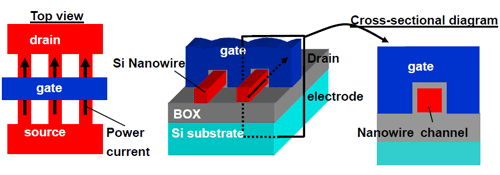 |
| Structure of a silicon nanowire transistor |
Abstract:
Increasing 75% on-state current by reducing parasitic resistance
Toshiba develops leading-edge silicon nanowire transistor for 16nm generation and beyond
Tokyo | Posted on June 15th, 2010Toshiba Corporation (TOKYO: 6502) today announced that it has developed a breakthrough technology for a nanowire transistor, a major candidate for a 3D structure transistor for system LSI in the 16nm generation and beyond. The company has achieved a 1mA/�m on-current, the world's highest level for a nanowire transistor, by reducing parasitic resistance and improving the on-current level by 75%. This is a major step towards practical application of nanowire transistors. This achievement will be presented at the 2010 Symposium on VLSI Technology in Hawaii, on June 17.
When the size of current planar transistors scales smaller, current leakage between the source and the drain at its off-stage (off-leakage) will become a critical problem in securing circuit reliability. To overcome this, transistors with a 3D structure, including silicon nanowire transistors, are being investigated as candidates for future generations of devices. The silicon nanowire transistor can suppress off-leakage and achieve further short-channel operation, because its thin wire-shaped silicon channel (nanowire channel) is effectively controlled by the surrounding gate. However, parasitic resistance in the nanowire-shaped source/drain, especially in the region under the gate sidewall, degrades the on-current.
Toshiba overcame this problem by optimizing gate fabrication and significantly reducing the thickness of the gate sidewall, from 30nm to 10nm. Low parasitic resistance was realized by epitaxial silicon growth on the source/drain with a thin gate sidewall, which leads to a 40% increase in on-current. The company also achieved a further 25% increase in current performance by changing the direction of the silicon nanowire channel from the <110> to <100> plane direction. Utilizing these technologies, Toshiba has demonstrated an industry-leading on-current level of 1mA/�m, when the off-current is 100nA/�m, a 75% increase in the on-current at the same off-current condition.
Toshiba will continue to promote development of the transistor towards establishing fundamental technologies for high-performance, low-power system LSIs.
This work was partly supported by New Energy and Industrial Technology Development Organization (NEDO) 's Development of Nanoelectronic Device Technology.
Information in the news releases, including product prices and specifications, content of services and contact information, is current on the date of the press announcement, but is subject to change without prior notice.
####
For more information, please click here
Copyright © Toshiba Corporation
If you have a comment, please Contact us.Issuers of news releases, not 7th Wave, Inc. or Nanotechnology Now, are solely responsible for the accuracy of the content.
Bookmark:


| Related News Press |
News and information
![]() Quantum computer improves AI predictions April 17th, 2026
Quantum computer improves AI predictions April 17th, 2026
![]() Flexible sensor gains sensitivity under pressure April 17th, 2026
Flexible sensor gains sensitivity under pressure April 17th, 2026
![]() A reusable chip for particulate matter sensing April 17th, 2026
A reusable chip for particulate matter sensing April 17th, 2026
![]() Detecting vibrational quantum beating in the predissociation dynamics of SF6 using time-resolved photoelectron spectroscopy April 17th, 2026
Detecting vibrational quantum beating in the predissociation dynamics of SF6 using time-resolved photoelectron spectroscopy April 17th, 2026
Govt.-Legislation/Regulation/Funding/Policy
![]() Quantum computer improves AI predictions April 17th, 2026
Quantum computer improves AI predictions April 17th, 2026
![]() Metasurfaces smooth light to boost magnetic sensing precision January 30th, 2026
Metasurfaces smooth light to boost magnetic sensing precision January 30th, 2026
![]() New imaging approach transforms study of bacterial biofilms August 8th, 2025
New imaging approach transforms study of bacterial biofilms August 8th, 2025
Chip Technology
![]() A reusable chip for particulate matter sensing April 17th, 2026
A reusable chip for particulate matter sensing April 17th, 2026
![]() Metasurfaces smooth light to boost magnetic sensing precision January 30th, 2026
Metasurfaces smooth light to boost magnetic sensing precision January 30th, 2026
Nanoelectronics
![]() Lab to industry: InSe wafer-scale breakthrough for future electronics August 8th, 2025
Lab to industry: InSe wafer-scale breakthrough for future electronics August 8th, 2025
![]() Interdisciplinary: Rice team tackles the future of semiconductors Multiferroics could be the key to ultralow-energy computing October 6th, 2023
Interdisciplinary: Rice team tackles the future of semiconductors Multiferroics could be the key to ultralow-energy computing October 6th, 2023
![]() Key element for a scalable quantum computer: Physicists from Forschungszentrum J�lich and RWTH Aachen University demonstrate electron transport on a quantum chip September 23rd, 2022
Key element for a scalable quantum computer: Physicists from Forschungszentrum J�lich and RWTH Aachen University demonstrate electron transport on a quantum chip September 23rd, 2022
![]() Reduced power consumption in semiconductor devices September 23rd, 2022
Reduced power consumption in semiconductor devices September 23rd, 2022
Announcements
![]() A fundamentally new therapeutic approach to cystic fibrosis: Nanobody repairs cellular defect April 17th, 2026
A fundamentally new therapeutic approach to cystic fibrosis: Nanobody repairs cellular defect April 17th, 2026
![]() UC Irvine physicists discover method to reverse �quantum scrambling� : The work addresses the problem of information loss in quantum computing system April 17th, 2026
UC Irvine physicists discover method to reverse �quantum scrambling� : The work addresses the problem of information loss in quantum computing system April 17th, 2026
Events/Classes
![]() Institute for Nanoscience hosts annual proposal planning meeting May 16th, 2025
Institute for Nanoscience hosts annual proposal planning meeting May 16th, 2025
![]() A New Blue: Mysterious origin of the ribbontail ray�s electric blue spots revealed July 5th, 2024
A New Blue: Mysterious origin of the ribbontail ray�s electric blue spots revealed July 5th, 2024
![]() Researchers demonstrate co-propagation of quantum and classical signals: Study shows that quantum encryption can be implemented in existing fiber networks January 20th, 2023
Researchers demonstrate co-propagation of quantum and classical signals: Study shows that quantum encryption can be implemented in existing fiber networks January 20th, 2023
|
|
||
|
|
||
| The latest news from around the world, FREE | ||
|
|
||
|
|
||
| Premium Products | ||
|
|
||
|
Only the news you want to read!
Learn More |
||
|
|
||
|
Full-service, expert consulting
Learn More |
||
|
|
||