Home > Press > Photonic Structures Fabrication in LiNbO3 Crystals using the System100 ICP180
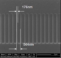 |
| Grating etched into LiNbO3 planar waveguides. The etched air gap width is 388 nm and depth is about 800nm |
Abstract:
Siyuan Yu, Professor in Photonics and Optical Communications
Department of Electrical & Electronic Engineering, University of Bristol
Photonic Structures Fabrication in LiNbO3 Crystals using the System100 ICP180
UK | Posted on June 14th, 2010The Photonics Group at the University of Bristol have used their OIPT System100 RIE100 ICP180 system to develop a high speed, high quality process for etching sub-micron features in Lithium Niobate (LiNbO3) and related materials. This work was motivated by the need to produce high aspect ratio, highly vertical features, such as photonic crystals, in LiNbO3.
LiNbO3 is a hard material to etch. Previously reported etch processes had limited dry etch rate of ~20 nm/min. Such slow etch rate was also typically associated with low selectivity over mask materials. Although the slow etch processes may be able to etch waveguides that does not require very vertical profiles, they require a long etch time. More importantly, they cannot be used to achieve photonic features with sizes approaching 100nm and requiring very smooth and vertical sidewall profiles to optimise their optical performance.
The Bristol group developed an optimised SF6-based chemistry on the RIE100/ICP180 system. The high density ICP plasma source enables etch rates of up to 200 nm/min, with vertical and smooth sidewalls. Ridge waveguides, gratings (Figure 1), and photonic crystals (Figure 2) have been successfully etched into LiNbO3 planar waveguide layers produced by proto exchange and by epitaxial growth on Lithium Tantalate (LiTaO3) substrates. Depths of up to 0.8 micron have been achieved with feature sizes of less than 200 nm.
The Bristol group have also been able to pattern the LiTaO3 substrate using such etching processes before the epitaxial growth of the LiNbO3 layer at Prof Pam Thomas' group in the Physics Department, Warwick University, who successfully produced buried photonic structures in these crystals.
####
For more information, please click here
Contacts:
Prof. Siyuan Yu.
Copyright © Oxford Instruments
If you have a comment, please Contact us.Issuers of news releases, not 7th Wave, Inc. or Nanotechnology Now, are solely responsible for the accuracy of the content.
Bookmark:


| Related News Press |
News and information
![]() Quantum computer improves AI predictions April 17th, 2026
Quantum computer improves AI predictions April 17th, 2026
![]() Flexible sensor gains sensitivity under pressure April 17th, 2026
Flexible sensor gains sensitivity under pressure April 17th, 2026
![]() A reusable chip for particulate matter sensing April 17th, 2026
A reusable chip for particulate matter sensing April 17th, 2026
![]() Detecting vibrational quantum beating in the predissociation dynamics of SF6 using time-resolved photoelectron spectroscopy April 17th, 2026
Detecting vibrational quantum beating in the predissociation dynamics of SF6 using time-resolved photoelectron spectroscopy April 17th, 2026
Possible Futures
![]() A fundamentally new therapeutic approach to cystic fibrosis: Nanobody repairs cellular defect April 17th, 2026
A fundamentally new therapeutic approach to cystic fibrosis: Nanobody repairs cellular defect April 17th, 2026
![]() UC Irvine physicists discover method to reverse �quantum scrambling� : The work addresses the problem of information loss in quantum computing system April 17th, 2026
UC Irvine physicists discover method to reverse �quantum scrambling� : The work addresses the problem of information loss in quantum computing system April 17th, 2026
Academic/Education
![]() Rice University launches Rice Synthetic Biology Institute to improve lives January 12th, 2024
Rice University launches Rice Synthetic Biology Institute to improve lives January 12th, 2024
![]() Multi-institution, $4.6 million NSF grant to fund nanotechnology training September 9th, 2022
Multi-institution, $4.6 million NSF grant to fund nanotechnology training September 9th, 2022
Announcements
![]() A fundamentally new therapeutic approach to cystic fibrosis: Nanobody repairs cellular defect April 17th, 2026
A fundamentally new therapeutic approach to cystic fibrosis: Nanobody repairs cellular defect April 17th, 2026
![]() UC Irvine physicists discover method to reverse �quantum scrambling� : The work addresses the problem of information loss in quantum computing system April 17th, 2026
UC Irvine physicists discover method to reverse �quantum scrambling� : The work addresses the problem of information loss in quantum computing system April 17th, 2026
Photonics/Optics/Lasers
![]() Metasurfaces smooth light to boost magnetic sensing precision January 30th, 2026
Metasurfaces smooth light to boost magnetic sensing precision January 30th, 2026
![]() From sensors to smart systems: the rise of AI-driven photonic noses January 30th, 2026
From sensors to smart systems: the rise of AI-driven photonic noses January 30th, 2026
|
|
||
|
|
||
| The latest news from around the world, FREE | ||
|
|
||
|
|
||
| Premium Products | ||
|
|
||
|
Only the news you want to read!
Learn More |
||
|
|
||
|
Full-service, expert consulting
Learn More |
||
|
|
||