Home > Press > Junctionless transistor outperforms nanowire MOSFET
 |
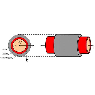
| Schematic representation of the cylindrical wrap-around gate nanowire |
Abstract:
The nanowire pinch-off field effect transistor (FET) or junctionless transistor is a uniformly doped nanowire without junctions with a wrap-around gate. The idea and basic working principle of the nanowire pinch-off transistor were developed in imec and already reported in 2007 and 2008. Recent modeling results obtained in imec for a GaAs and Si nanowire indicate that the nanowire pinch-off FET can outperform the nanowire MOSFET. These results combined with scalability and ease of processing make the junctionless transistor a true competitor for the nanowire MOSFET.
Junctionless transistor outperforms nanowire MOSFET
The Netherlands | Posted on April 21st, 2010Several years ago, imec theoreticians developed the concept of the pinch-off nanowire FET. Originally, the idea was to avoid surface interactions such as surface roughness scattering or high-k surface phonon scattering wich degrade the charge carrier mobility, by moving the charge carriers away from the interface between the substrate and the insulator. The solution to this problem was to consider a nanowire where source, drain and channel are uniformly doped. For a n-type nanowire pinch-off FET, the charge carriers responsible for the current are delivered by the ionized donors. As the gate voltage is increased, the channel of the wire is depleted and, eventually, pinch-off will occur.
More detailed results about the idea and basic working principle of the nanowire pinch-off FET as proposed by imec can be found in:
[1] Sor�e, B.; Magnus, W.; Pourtois, G. Analytical and self-consistent quantum mechanical model for a JFET nanowire. In: IWCE12. 2007. (8-10 October 2007; Amherst, NJ, USA.)
[2] Sor�e, B.; Magnus, W.; Pourtois, G. Analytical and self-consistent quantum mechanical model for a surrounding gate MOS nanowire operated in JFET mode. JCEL. Vol. 7: (3) 380-383; 2008.
####
About imec
Imec is Europe�s largest independent research center in nanoelectronics and nano-technology. Its staff of more than 1,750 people includes over 550 industrial residents and guest researchers. Imec�s research is applied in better healthcare, smart electronics, sustainable energy, and safer transport.
For more information, please click here
Copyright © imec
If you have a comment, please Contact us.Issuers of news releases, not 7th Wave, Inc. or Nanotechnology Now, are solely responsible for the accuracy of the content.
| Related News Press |
News and information
![]() Quantum computer improves AI predictions April 17th, 2026
Quantum computer improves AI predictions April 17th, 2026
![]() Flexible sensor gains sensitivity under pressure April 17th, 2026
Flexible sensor gains sensitivity under pressure April 17th, 2026
![]() A reusable chip for particulate matter sensing April 17th, 2026
A reusable chip for particulate matter sensing April 17th, 2026
![]() Detecting vibrational quantum beating in the predissociation dynamics of SF6 using time-resolved photoelectron spectroscopy April 17th, 2026
Detecting vibrational quantum beating in the predissociation dynamics of SF6 using time-resolved photoelectron spectroscopy April 17th, 2026
Chip Technology
![]() A reusable chip for particulate matter sensing April 17th, 2026
A reusable chip for particulate matter sensing April 17th, 2026
![]() Metasurfaces smooth light to boost magnetic sensing precision January 30th, 2026
Metasurfaces smooth light to boost magnetic sensing precision January 30th, 2026
Nanoelectronics
![]() Lab to industry: InSe wafer-scale breakthrough for future electronics August 8th, 2025
Lab to industry: InSe wafer-scale breakthrough for future electronics August 8th, 2025
![]() Interdisciplinary: Rice team tackles the future of semiconductors Multiferroics could be the key to ultralow-energy computing October 6th, 2023
Interdisciplinary: Rice team tackles the future of semiconductors Multiferroics could be the key to ultralow-energy computing October 6th, 2023
![]() Key element for a scalable quantum computer: Physicists from Forschungszentrum J�lich and RWTH Aachen University demonstrate electron transport on a quantum chip September 23rd, 2022
Key element for a scalable quantum computer: Physicists from Forschungszentrum J�lich and RWTH Aachen University demonstrate electron transport on a quantum chip September 23rd, 2022
![]() Reduced power consumption in semiconductor devices September 23rd, 2022
Reduced power consumption in semiconductor devices September 23rd, 2022
Announcements
![]() A fundamentally new therapeutic approach to cystic fibrosis: Nanobody repairs cellular defect April 17th, 2026
A fundamentally new therapeutic approach to cystic fibrosis: Nanobody repairs cellular defect April 17th, 2026
![]() UC Irvine physicists discover method to reverse �quantum scrambling� : The work addresses the problem of information loss in quantum computing system April 17th, 2026
UC Irvine physicists discover method to reverse �quantum scrambling� : The work addresses the problem of information loss in quantum computing system April 17th, 2026
|
|
||
|
|
||
| The latest news from around the world, FREE | ||
|
|
||
|
|
||
| Premium Products | ||
|
|
||
|
Only the news you want to read!
Learn More |
||
|
|
||
|
Full-service, expert consulting
Learn More |
||
|
|
||


