Home > Press > Graphene and gallium arsenide: two perfect partners find each other
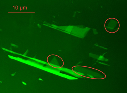 |
| The normally practically invisible single-carbon-atom layers can be made visible under a normal light (optical) microscope, if the support (layer) is designed as an anti-reflection filter. Single-layer graphene was identified inside the markings. |
Abstract:
PTB has for the first time made graphene visible on gallium arsenide - A successful combination of two unique electronic materials
Graphene and gallium arsenide: two perfect partners find each other
Berlin | Posted on September 21st, 2009It is the marriage of two top candidates for the electronics of the future, both excentric and extremely interesting: Graphene, one of the partners, is an extremely thin fellow and besides, very young. Not until 2004 was it possible to specifically produce and investigate the single layer of carbon atoms. Its electronic properties are remarkable, because, among other things, its electrons can move so tremendously fast. It is a perfect partner for gallium arsenide, the semiconductor that allows tailoring of its electrical properties and which is the starting material of the fastest electrical and opto-electronic components. Besides, it is possible to produce gallium arsenide with an atomic-layer-smooth surface; this should suit well as a support for graphene. Scientists of the Physikalisch-Technische Bundesanstalt (PTB) have now, with the aid of a special design, succeeded in making graphene visible on gallium arsenide. Previously it has only been possible on silicon oxide. Now that they are able to view with a light optical microscope the graphene layer, which is thinner than one thousandth of a light wavelength, the researchers want to measure the electrical properties of their new material combination. As experts for precision measurements, the PTB physicists are thus especially well equipped to do this.
They use the principle of the anti-reflective layer: If on a material one superimposes a very thin, nearly transparent layer of another material, then the reflectivity of the lower layer changes clearly visibly. In order to make their lower layer of gallium arsenide (plus graphene atomic layer) visible, the PTB physicists chose aluminium arsenide (AlAs). However, it is so similar to gallium arsenide (GaAs) in its optical properties that they had to employ a few tricks: They vapour-coated not only one, but rather several wafer-thin layers. "Thus, even with optically similar materials it is possible, in a manner of speaking, to 'grow' interference effects", Dr. Franz-Josef Ahlers, the responsible department head at PTB, explained. "This principle is known from optical interference filters. We have adapted it for our purposes".
First of all, he and his colleagues calculated the optical properties of different GaAs and AlAs layers and optimized the layer sequence such that they could expect a sufficiently good detectability of graphene. Following this recipe, they got down to action and with the molecular beam epitaxial facility of PTB accurately produced a corresponding GaAs/AlAs crystal atom layer. Then in the same procedure as with silicon oxide, it was overlaid with graphite fragments. "Different from silicon but as predicted by the calculation, although single carbon layers are no longer visible at all wavelengths of visible light, it is, however, possible, e.g. with a simple green filter, to limit the wavelength range such that the graphene is easily visible", explained Ahlers. In the photo, all lighter areas of the dark GaAs are covered with graphene. From the degree of lightening it is possible to conclude the number of individual layers of atoms. The marked areas are 'real', that is, single-layer graphene. But next to them, there are also two, three and multiple layers of carbon atoms, which also have interesting properties. This arrangement was confirmed again with another method, Raman spectroscopy.
Following such a simple identification with a normal light optical microscope, the further steps in the manufacture of electrical components from graphene surfaces are now possible without any difficulty. Thus the PTB scientists can now begin to accurately measure the electrical properties of the new material combination.
The original publication:
Graphene on Gallium Arsenide: Engineering the visibility.
M. Friedemann, K. Pierz, R. Stosch, F. J. Ahlers.
Applied Physics Letters, Appl. Phys. Lett. 95,
DOI: 10.1063/1.3224910,
link.aip.org/link/?APL/95/102103
####
About Physikalisch-Technische Bundesanstalt
The Physikalisch-Technische Bundesanstalt (PTB) is the national metrology institute providing scientific and technical services. PTB measures with the highest accuracy and reliability � metrology as the core competence.
For more information, please click here
Contacts:
Dr. Franz Josef Ahlers, PTB Department 2.6 Quantum Electrical Metrology,
phone: +49 531 592 2600,
Copyright © Physikalisch-Technische Bundesanstalt
If you have a comment, please Contact us.Issuers of news releases, not 7th Wave, Inc. or Nanotechnology Now, are solely responsible for the accuracy of the content.
Bookmark:


| Related News Press |
News and information
![]() Quantum computer improves AI predictions April 17th, 2026
Quantum computer improves AI predictions April 17th, 2026
![]() Flexible sensor gains sensitivity under pressure April 17th, 2026
Flexible sensor gains sensitivity under pressure April 17th, 2026
![]() A reusable chip for particulate matter sensing April 17th, 2026
A reusable chip for particulate matter sensing April 17th, 2026
![]() Detecting vibrational quantum beating in the predissociation dynamics of SF6 using time-resolved photoelectron spectroscopy April 17th, 2026
Detecting vibrational quantum beating in the predissociation dynamics of SF6 using time-resolved photoelectron spectroscopy April 17th, 2026
Chemistry
![]() Projecting light to dispense liquids: A new route to ultra-precise microdroplets January 30th, 2026
Projecting light to dispense liquids: A new route to ultra-precise microdroplets January 30th, 2026
![]() From sensors to smart systems: the rise of AI-driven photonic noses January 30th, 2026
From sensors to smart systems: the rise of AI-driven photonic noses January 30th, 2026
![]() "Nanoreactor" cage uses visible light for catalytic and ultra-selective cross-cycloadditions October 3rd, 2025
"Nanoreactor" cage uses visible light for catalytic and ultra-selective cross-cycloadditions October 3rd, 2025
![]() Cambridge chemists discover simple way to build bigger molecules � one carbon at a time June 6th, 2025
Cambridge chemists discover simple way to build bigger molecules � one carbon at a time June 6th, 2025
Possible Futures
![]() A fundamentally new therapeutic approach to cystic fibrosis: Nanobody repairs cellular defect April 17th, 2026
A fundamentally new therapeutic approach to cystic fibrosis: Nanobody repairs cellular defect April 17th, 2026
![]() UC Irvine physicists discover method to reverse �quantum scrambling� : The work addresses the problem of information loss in quantum computing system April 17th, 2026
UC Irvine physicists discover method to reverse �quantum scrambling� : The work addresses the problem of information loss in quantum computing system April 17th, 2026
Nanoelectronics
![]() Lab to industry: InSe wafer-scale breakthrough for future electronics August 8th, 2025
Lab to industry: InSe wafer-scale breakthrough for future electronics August 8th, 2025
![]() Interdisciplinary: Rice team tackles the future of semiconductors Multiferroics could be the key to ultralow-energy computing October 6th, 2023
Interdisciplinary: Rice team tackles the future of semiconductors Multiferroics could be the key to ultralow-energy computing October 6th, 2023
![]() Key element for a scalable quantum computer: Physicists from Forschungszentrum J�lich and RWTH Aachen University demonstrate electron transport on a quantum chip September 23rd, 2022
Key element for a scalable quantum computer: Physicists from Forschungszentrum J�lich and RWTH Aachen University demonstrate electron transport on a quantum chip September 23rd, 2022
![]() Reduced power consumption in semiconductor devices September 23rd, 2022
Reduced power consumption in semiconductor devices September 23rd, 2022
Discoveries
![]() Quantum computer improves AI predictions April 17th, 2026
Quantum computer improves AI predictions April 17th, 2026
![]() Flexible sensor gains sensitivity under pressure April 17th, 2026
Flexible sensor gains sensitivity under pressure April 17th, 2026
![]() A reusable chip for particulate matter sensing April 17th, 2026
A reusable chip for particulate matter sensing April 17th, 2026
![]() Detecting vibrational quantum beating in the predissociation dynamics of SF6 using time-resolved photoelectron spectroscopy April 17th, 2026
Detecting vibrational quantum beating in the predissociation dynamics of SF6 using time-resolved photoelectron spectroscopy April 17th, 2026
Announcements
![]() A fundamentally new therapeutic approach to cystic fibrosis: Nanobody repairs cellular defect April 17th, 2026
A fundamentally new therapeutic approach to cystic fibrosis: Nanobody repairs cellular defect April 17th, 2026
![]() UC Irvine physicists discover method to reverse �quantum scrambling� : The work addresses the problem of information loss in quantum computing system April 17th, 2026
UC Irvine physicists discover method to reverse �quantum scrambling� : The work addresses the problem of information loss in quantum computing system April 17th, 2026
Tools
![]() Metasurfaces smooth light to boost magnetic sensing precision January 30th, 2026
Metasurfaces smooth light to boost magnetic sensing precision January 30th, 2026
![]() From sensors to smart systems: the rise of AI-driven photonic noses January 30th, 2026
From sensors to smart systems: the rise of AI-driven photonic noses January 30th, 2026
![]() Japan launches fully domestically produced quantum computer: Expo visitors to experience quantum computing firsthand August 8th, 2025
Japan launches fully domestically produced quantum computer: Expo visitors to experience quantum computing firsthand August 8th, 2025
|
|
||
|
|
||
| The latest news from around the world, FREE | ||
|
|
||
|
|
||
| Premium Products | ||
|
|
||
|
Only the news you want to read!
Learn More |
||
|
|
||
|
Full-service, expert consulting
Learn More |
||
|
|
||