Home > Press > IBM Scientists Effectively Eliminate Wear at the Nanoscale
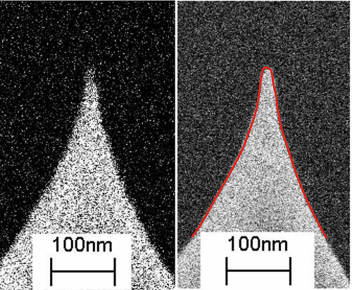 |
| Scanning electron micrograph showing no measurable mechanical wear in a vibrating nanotip sliding 750-meters over a polymer surface. The tip measures 500 nanometers in length and only 5 nanometers at its apex. On the left is the original tip, on the right the same tip after the 750-meter wear test. The red line shows the outline of the original tip shape overlayed on an image taken at the end of the experiment. The key to success: A small almost imperceptible vibration of the tip. Image courtesy of IBM Research - Zurich |
Abstract:
Results could lead to new high-precision and high-quality nanomechanical tools in nanofabrication and in the development of next-generations chips
IBM Scientists Effectively Eliminate Wear at the Nanoscale
Zurich, Switzerland | Posted on September 8th, 2009IBM (NYSE: IBM) scientists have demonstrated a promising and practical method that effectively eliminates the mechanical wear in the nanometer-sharp tips used in scanning probe-based techniques. This discovery can potentially be used in the development of next generation, more advanced computer chips that have higher performance and smaller feature sizes. Scanning probe-based tools could be one approach to extend the capabilities, quality and precision beyond the projected limits of current production and characterization tools.
Scanning probe-based techniques utilize tiny, nanometer-sharp tips borrowed from atomic force microscopy to manipulate nanostructures and devices by scanning or rather sliding in very close proximity over the surface�similar to the way the needle of a record player on a record. Today, these techniques�including for example the well-known atomic force microscope�are established tools for scientists to explore the nanocosmos. Scanning-probe techniques today allow for the highest possible resolution down to the atomic or molecular scale and represent essentially the scientists' "eyes", "ears", "nose", and "hands" as they explore the smallest objects known to mankind.
In the semiconductor industry, these techniques due to their atomic resolution and manipulation capabilities become increasingly attractive for use in the development and manufacturing of next generation chips with ultra-small feature sizes. While small by most standards, today's 40 nm transistors can still shrink further, but it becomes increasingly challenging and costly since the current tools and methods to develop and process the chips out of silicon wafers approach physical limitations for critical chip layers.
"Continued scaling to further increase device performance will require new device architectures, smaller feature sizes and new materials. Tools based on scanning probe technology could become essential for the metrology of future technology nodes as well as for the development, fabrication and characterization of novel nanoscale devices," says IBM Fellow Evangelos Eleftheriou of IBM Research - Zurich.
A key limiting factor for the prospects of large-scale industrial uses of such techniques, however, has been mechanical wear of the sharp tips. Wear resulting from friction between moving parts are inherent to all mechanical processes on the macro- as well as on the nanometer-scale. However, for scanning probe-based technologies, which rely on a nanometer-sharp tip�measuring just five nanometers at its apex�this problem is accentuated. A few cubic nanometers more or less can ruin the sensitivity of the tip. "In future industrial applications such as large area characterization of the features on a silicon wafer, a tip would need to be able to slide tens of kilometers or miles without replacement," explains IBM scientist Mark Lantz. In the currently used scanning modes, the tip wears out after a few meters or yards. "Moreover, in addition to causing wear of the tip, friction can potentially also do damage to the surface being characterized."
In their paper, published in the September issue of Nature Nanotechnology, IBM scientists solve this challenge by "demonstrating the effective elimination of wear on a tip sliding on a polymer surface over a distance of 750 meters by modulating the force acting on the tip-sample contact." By applying an AC voltage between the cantilever�the mechanical arms on which the tips are attached and over which they are controlled�and the sample surface, the cantilever can be excited at high frequencies of one Megahertz. The cantilever bends and the tip vibrates with an almost imperceptible estimated amplitude of one nanometer. "Though vanishingly small, it is this vibration that greatly reduces friction and "effectively" eliminates�to below the detection limit corresponding to the remarkable low number of losing one atom per meter�tip wear under experimental conditions," states Bernd Gotsmann of IBM Research - Zurich. After the 750-meter wear test, which took a week of continuous operation, the tip was still operating flawlessly.
With the wear problem tackled, researchers at IBM Research - Zurich are now investigating a number of possible applications of scanning probe-based technologies including nanofabrication, nanolithography and high-speed metrology. Operating a large number of tips in parallel would enable, high-throughput, high-speed, automated metrology systems for potential use in chip development and manufacturing. Such metrology systems could characterize device dimensions or identify defects on the structured silicon wafers with much higher precision and accuracy and potentially lower cost than currently available tools. Scientists at IBM Research - Zurich are also investigating powerful scanning probe-based method for high speed patterning of complex two and three-dimensional nanoscale structures.
The scientific paper entitled "Dynamic Superlubricity and the Elimination of Wear on the Nanoscale" by M.A. Lantz, D. Wiesmann, and B. Gotsmann, is published in Nature Nanotechnology, Volume 4, Issue 9 (September 2009).
####
For more information, please click here
Contacts:
Nicole Herfurth
Media Relations
IBM Research GmbH
IBM Research - Zurich
S�umerstrasse 4
8803 R�schlikon
Switzerland
Tel +41 44 724 8445
Fax +41 44 724 8952
Copyright © http://www.zurich.ibm.com
If you have a comment, please Contact us.Issuers of news releases, not 7th Wave, Inc. or Nanotechnology Now, are solely responsible for the accuracy of the content.
Bookmark:


| Related News Press |
News and information
![]() Quantum computer improves AI predictions April 17th, 2026
Quantum computer improves AI predictions April 17th, 2026
![]() Flexible sensor gains sensitivity under pressure April 17th, 2026
Flexible sensor gains sensitivity under pressure April 17th, 2026
![]() A reusable chip for particulate matter sensing April 17th, 2026
A reusable chip for particulate matter sensing April 17th, 2026
![]() Detecting vibrational quantum beating in the predissociation dynamics of SF6 using time-resolved photoelectron spectroscopy April 17th, 2026
Detecting vibrational quantum beating in the predissociation dynamics of SF6 using time-resolved photoelectron spectroscopy April 17th, 2026
Possible Futures
![]() A fundamentally new therapeutic approach to cystic fibrosis: Nanobody repairs cellular defect April 17th, 2026
A fundamentally new therapeutic approach to cystic fibrosis: Nanobody repairs cellular defect April 17th, 2026
![]() UC Irvine physicists discover method to reverse �quantum scrambling� : The work addresses the problem of information loss in quantum computing system April 17th, 2026
UC Irvine physicists discover method to reverse �quantum scrambling� : The work addresses the problem of information loss in quantum computing system April 17th, 2026
Chip Technology
![]() A reusable chip for particulate matter sensing April 17th, 2026
A reusable chip for particulate matter sensing April 17th, 2026
![]() Metasurfaces smooth light to boost magnetic sensing precision January 30th, 2026
Metasurfaces smooth light to boost magnetic sensing precision January 30th, 2026
Nanotubes/Buckyballs/Fullerenes/Nanorods/Nanostrings/Nanosheets
![]() Tiny nanosheets, big leap: A new sensor detects ethanol at ultra-low levels January 30th, 2026
Tiny nanosheets, big leap: A new sensor detects ethanol at ultra-low levels January 30th, 2026
![]() Enhancing power factor of p- and n-type single-walled carbon nanotubes April 25th, 2025
Enhancing power factor of p- and n-type single-walled carbon nanotubes April 25th, 2025
![]() Chainmail-like material could be the future of armor: First 2D mechanically interlocked polymer exhibits exceptional flexibility and strength January 17th, 2025
Chainmail-like material could be the future of armor: First 2D mechanically interlocked polymer exhibits exceptional flexibility and strength January 17th, 2025
![]() Innovative biomimetic superhydrophobic coating combines repair and buffering properties for superior anti-erosion December 13th, 2024
Innovative biomimetic superhydrophobic coating combines repair and buffering properties for superior anti-erosion December 13th, 2024
Nanoelectronics
![]() Lab to industry: InSe wafer-scale breakthrough for future electronics August 8th, 2025
Lab to industry: InSe wafer-scale breakthrough for future electronics August 8th, 2025
![]() Interdisciplinary: Rice team tackles the future of semiconductors Multiferroics could be the key to ultralow-energy computing October 6th, 2023
Interdisciplinary: Rice team tackles the future of semiconductors Multiferroics could be the key to ultralow-energy computing October 6th, 2023
![]() Key element for a scalable quantum computer: Physicists from Forschungszentrum J�lich and RWTH Aachen University demonstrate electron transport on a quantum chip September 23rd, 2022
Key element for a scalable quantum computer: Physicists from Forschungszentrum J�lich and RWTH Aachen University demonstrate electron transport on a quantum chip September 23rd, 2022
![]() Reduced power consumption in semiconductor devices September 23rd, 2022
Reduced power consumption in semiconductor devices September 23rd, 2022
Discoveries
![]() Quantum computer improves AI predictions April 17th, 2026
Quantum computer improves AI predictions April 17th, 2026
![]() Flexible sensor gains sensitivity under pressure April 17th, 2026
Flexible sensor gains sensitivity under pressure April 17th, 2026
![]() A reusable chip for particulate matter sensing April 17th, 2026
A reusable chip for particulate matter sensing April 17th, 2026
![]() Detecting vibrational quantum beating in the predissociation dynamics of SF6 using time-resolved photoelectron spectroscopy April 17th, 2026
Detecting vibrational quantum beating in the predissociation dynamics of SF6 using time-resolved photoelectron spectroscopy April 17th, 2026
Announcements
![]() A fundamentally new therapeutic approach to cystic fibrosis: Nanobody repairs cellular defect April 17th, 2026
A fundamentally new therapeutic approach to cystic fibrosis: Nanobody repairs cellular defect April 17th, 2026
![]() UC Irvine physicists discover method to reverse �quantum scrambling� : The work addresses the problem of information loss in quantum computing system April 17th, 2026
UC Irvine physicists discover method to reverse �quantum scrambling� : The work addresses the problem of information loss in quantum computing system April 17th, 2026
Tools
![]() Metasurfaces smooth light to boost magnetic sensing precision January 30th, 2026
Metasurfaces smooth light to boost magnetic sensing precision January 30th, 2026
![]() From sensors to smart systems: the rise of AI-driven photonic noses January 30th, 2026
From sensors to smart systems: the rise of AI-driven photonic noses January 30th, 2026
![]() Japan launches fully domestically produced quantum computer: Expo visitors to experience quantum computing firsthand August 8th, 2025
Japan launches fully domestically produced quantum computer: Expo visitors to experience quantum computing firsthand August 8th, 2025
|
|
||
|
|
||
| The latest news from around the world, FREE | ||
|
|
||
|
|
||
| Premium Products | ||
|
|
||
|
Only the news you want to read!
Learn More |
||
|
|
||
|
Full-service, expert consulting
Learn More |
||
|
|
||