Home > Press > World’s First Proven Ultrasound Holographic Imaging Allows Correction of Nanoscale Subsurface Defects, Spurs Spin-off Company from SRC Work with North
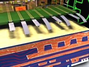 |
| New sub-surface, embedded defect analysis will be more accurate than any other imaging process, spurring a spin-off company to commercialize the technology. (Photo: Business Wire) |
Abstract:
New innovation to help enable semiconductor and pharmaceutical industries to evaluate and influence vital ultra-small structures
World’s First Proven Ultrasound Holographic Imaging Allows Correction of Nanoscale Subsurface Defects, Spurs Spin-off Company from SRC Work with North
Research Triangle Park, NC | Posted on March 4th, 2009Just as x-ray technology, MRI and sonography transformed the practice of medicine, a newly created approach for seeing the invisible promises great potential for finding new ways to improve the health of human and microelectronic patients alike. Semiconductor Research Corporation (SRC), the world's leading university-research consortium for semiconductors and related technologies, today joined with Northwestern University to announce successful demonstration of a unique ultrasound holography approach that enables scientists to view the tiniest of buried structures.
The resulting three-dimensional information will provide benefits ranging from greater yields for semiconductor manufacturers to more effective treatments for medical patients.
Using a novel, non-destructive approach that combines, for the first time ever, scanning-probe microscopy (SPM) with ultrasound and holography, researchers at Northwestern University have demonstrated the ability to view subsurface particles as small as 15-20 nanometers (a nanometer is one billionth of a meter). Such capabilities have not previously been possible without slicing the sample, which changes both the composition and structure and sacrifices characteristics of the studied subject.
What makes the new approach revolutionary is the combined use of the SPM, ultrasound and holography. SPM offers nanoscale resolution. Ultrasound is non-destructive, transparent to all materials and sensitive to embedded structures, including nano-sized defects. Holography also can provide sophisticated three-dimensional representations of the buried information. Together, the three technologies offer unprecedented visibility to the increasingly important tiny parts of nature.
As there's neither a similar approach nor such a high class of result available anywhere, a high-tech start-up company has been launched to further the commercial applications for these methods. Named NanoSonix Inc., the spin-off will develop a nanoscale-imaging toolset capable of rapid evaluation of defects and flaws below the surfaces as well as valuable recognition of buried patterns and structures.
"Microelectronics, in particular, is a flaw-intolerant technology where even nanoscale defects can compromise the performance and yield of the devices," said Dr. Dan Herr, director of nanomanufacturing sciences for SRC-GRC, an entity of SRC. "The ability to see such defects is critical for yield enhancement as devices become smaller and such metrology techniques and tools become even more crucial. These results are very good news for multiple industries."
Utilizing the new technology, the microelectronics and nano-electro-mechanical systems (NEMS) industries can improve performance of their devices, time to yield and, ultimately, yield rates by deploying this technique in process development and as an in-line quality control tool. Thanks to the non-destructive imaging approach, the pharmaceutical industry should benefit from better understanding of how drugs distribute, accumulate and clear from different parts of the body.
"Biomedicine is moving towards use of nano-bio-structures to interrogate cells and deliver therapeutic cargo. This requires a non-invasive view inside the cells to monitor what's happening under physiologically viable conditions," said Dr. Vinayak Dravid, professor of materials science and engineering and the director of the NUANCE Center at Northwestern University. "With the new imaging technology, it's possible to sharply increase our understanding of the bio-distribution of new drugs and the important interactions of nanoparticles and cells during intended or desirable therapeutic delivery or unintended environmental uptake."
Next steps in development of the technology include system integration, material handling, faster scanning and high through-put of results. In-line tools and methods for addressing these needs will be created by NanoSonix. For instance, in the next 12 months, the spin-off will develop an add-on module for existing commercial SPM equipment in order to meet associated off-line metrology requirements. Availability of such an add-on module will make this technology accessible to a wider community, not only in semiconductor metrology but also in bio-application for both academia and industry to look deep below surfaces non-destructively with nanoscale resolution.
####
About SRC-GRC
Global Research Collaboration (GRC) is one of three research program entities of SRC. Celebrating 27 years of collaborative research for the semiconductor industry, SRC defines industry needs, invests in and manages the research that gives its members a competitive advantage in the dynamic global marketplace. Awarded the National Medal of Technology, America’s highest recognition for contributions to technology, SRC expands the industry knowledge base and attracts premier students to help innovate and transfer semiconductor technology to the commercial industry.
For more information, please click here
Contacts:
SRC (Cardinal Communications)
Scott Stevens, +1-512-413-9540
Copyright © Business Wire 2009
If you have a comment, please Contact us.Issuers of news releases, not 7th Wave, Inc. or Nanotechnology Now, are solely responsible for the accuracy of the content.
Bookmark:


| Related News Press |
News and information
![]() Quantum computer improves AI predictions April 17th, 2026
Quantum computer improves AI predictions April 17th, 2026
![]() Flexible sensor gains sensitivity under pressure April 17th, 2026
Flexible sensor gains sensitivity under pressure April 17th, 2026
![]() A reusable chip for particulate matter sensing April 17th, 2026
A reusable chip for particulate matter sensing April 17th, 2026
![]() Detecting vibrational quantum beating in the predissociation dynamics of SF6 using time-resolved photoelectron spectroscopy April 17th, 2026
Detecting vibrational quantum beating in the predissociation dynamics of SF6 using time-resolved photoelectron spectroscopy April 17th, 2026
Imaging
![]() Simple algorithm paired with standard imaging tool could predict failure in lithium metal batteries August 8th, 2025
Simple algorithm paired with standard imaging tool could predict failure in lithium metal batteries August 8th, 2025
Chip Technology
![]() A reusable chip for particulate matter sensing April 17th, 2026
A reusable chip for particulate matter sensing April 17th, 2026
![]() Metasurfaces smooth light to boost magnetic sensing precision January 30th, 2026
Metasurfaces smooth light to boost magnetic sensing precision January 30th, 2026
Nanomedicine
![]() A fundamentally new therapeutic approach to cystic fibrosis: Nanobody repairs cellular defect April 17th, 2026
A fundamentally new therapeutic approach to cystic fibrosis: Nanobody repairs cellular defect April 17th, 2026
![]() New molecular technology targets tumors and simultaneously silences two ‘undruggable’ cancer genes August 8th, 2025
New molecular technology targets tumors and simultaneously silences two ‘undruggable’ cancer genes August 8th, 2025
![]() New imaging approach transforms study of bacterial biofilms August 8th, 2025
New imaging approach transforms study of bacterial biofilms August 8th, 2025
![]() Electrifying results shed light on graphene foam as a potential material for lab grown cartilage June 6th, 2025
Electrifying results shed light on graphene foam as a potential material for lab grown cartilage June 6th, 2025
Discoveries
![]() Quantum computer improves AI predictions April 17th, 2026
Quantum computer improves AI predictions April 17th, 2026
![]() Flexible sensor gains sensitivity under pressure April 17th, 2026
Flexible sensor gains sensitivity under pressure April 17th, 2026
![]() A reusable chip for particulate matter sensing April 17th, 2026
A reusable chip for particulate matter sensing April 17th, 2026
![]() Detecting vibrational quantum beating in the predissociation dynamics of SF6 using time-resolved photoelectron spectroscopy April 17th, 2026
Detecting vibrational quantum beating in the predissociation dynamics of SF6 using time-resolved photoelectron spectroscopy April 17th, 2026
Announcements
![]() A fundamentally new therapeutic approach to cystic fibrosis: Nanobody repairs cellular defect April 17th, 2026
A fundamentally new therapeutic approach to cystic fibrosis: Nanobody repairs cellular defect April 17th, 2026
![]() UC Irvine physicists discover method to reverse ‘quantum scrambling’ : The work addresses the problem of information loss in quantum computing system April 17th, 2026
UC Irvine physicists discover method to reverse ‘quantum scrambling’ : The work addresses the problem of information loss in quantum computing system April 17th, 2026
Tools
![]() Metasurfaces smooth light to boost magnetic sensing precision January 30th, 2026
Metasurfaces smooth light to boost magnetic sensing precision January 30th, 2026
![]() From sensors to smart systems: the rise of AI-driven photonic noses January 30th, 2026
From sensors to smart systems: the rise of AI-driven photonic noses January 30th, 2026
![]() Japan launches fully domestically produced quantum computer: Expo visitors to experience quantum computing firsthand August 8th, 2025
Japan launches fully domestically produced quantum computer: Expo visitors to experience quantum computing firsthand August 8th, 2025
Alliances/Trade associations/Partnerships/Distributorships
![]() Chicago Quantum Exchange welcomes six new partners highlighting quantum technology solutions, from Chicago and beyond September 23rd, 2022
Chicago Quantum Exchange welcomes six new partners highlighting quantum technology solutions, from Chicago and beyond September 23rd, 2022
![]() University of Illinois Chicago joins Brookhaven Lab's Quantum Center June 10th, 2022
University of Illinois Chicago joins Brookhaven Lab's Quantum Center June 10th, 2022
|
|
||
|
|
||
| The latest news from around the world, FREE | ||
|
|
||
|
|
||
| Premium Products | ||
|
|
||
|
Only the news you want to read!
Learn More |
||
|
|
||
|
Full-service, expert consulting
Learn More |
||
|
|
||