Home > Press > Research advances nanowire technology for large-scale applications
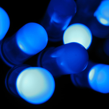 |
| LED lights Photo: � iPhoto/kr7ysztof |
Abstract:
Researchers at Northeastern created a network of nanowires that can be scaled up more efficiently and cost-effectively to create displays such as the NASDAQ sign in New York City's Times Square.
Using Gallium nitride (GaN), a highly effective semiconductor material, the team created, for the first time, a horizontally aligned network of GaN nanowires, which are integral components in the development of electrical circuits in the nanoscale. GaN is currently used to create light-emitting diodes (LED) and blue and ultra-violet emitting lasers.
Research advances nanowire technology for large-scale applications
Boston, MA | Posted on February 26th, 2009
Photo: � iPhoto/kr7ysztof
February 26, 2009
Researchers at Northeastern created a network of nanowires that can be scaled up more efficiently and cost-effectively to create displays such as the NASDAQ sign in New York City's Times Square.
Using Gallium nitride (GaN), a highly effective semiconductor material, the team created, for the first time, a horizontally aligned network of GaN nanowires, which are integral components in the development of electrical circuits in the nanoscale. GaN is currently used to create light-emitting diodes (LED) and blue and ultra-violet emitting lasers.
"Making devices that emit blue light and ultra-violet light is currently very expensive," said Latika Menon, assistant professor of physics and co-author of the study. "The horizontal structure of the GaN nanowire network will result in a more cost-effective way to advance this technology."
Electrodes allow for the flow of electricity between GaN nanowires and electrical wires, and the horizontal structure of the GaN nanowire networks are more easily attached to electrodes than vertical networks. In addition, the GaN nanowires have a cubic structure, with optical and transport properties that are more advanced than other nanowire structures, resulting in a more effective electrical circuit.
In terms of manufacturing, these horizontal network patterns can also be scaled up to large wafer sizes that are more compatible with the technology used to integrate them into new nanoelectronic devices. These devices connect nanotechnology and electronic devices to develop smaller and less costly manufacturing processes and products.
The research, published in a recent issue of the "Journal of Materials Chemistry," was funded by the National Science Foundation (NSF) and the NSF Nanoscale Science and Engineering Center for High-rate Nanomanufacturing at Northeastern. Other Northeastern researchers participating in this project include physicist Zhen Wu, as well as Myung Gwan Hahm and Yung Joon Jung from the department of mechanical and electrical engineering.
####
For more information, please click here
Contacts:
Jenny Catherine Eriksen
617-373-2802
Copyright © Northeastern University
If you have a comment, please Contact us.Issuers of news releases, not 7th Wave, Inc. or Nanotechnology Now, are solely responsible for the accuracy of the content.
Bookmark:


| Related News Press |
News and information
![]() Quantum computer improves AI predictions April 17th, 2026
Quantum computer improves AI predictions April 17th, 2026
![]() Flexible sensor gains sensitivity under pressure April 17th, 2026
Flexible sensor gains sensitivity under pressure April 17th, 2026
![]() A reusable chip for particulate matter sensing April 17th, 2026
A reusable chip for particulate matter sensing April 17th, 2026
![]() Detecting vibrational quantum beating in the predissociation dynamics of SF6 using time-resolved photoelectron spectroscopy April 17th, 2026
Detecting vibrational quantum beating in the predissociation dynamics of SF6 using time-resolved photoelectron spectroscopy April 17th, 2026
Display technology/LEDs/SS Lighting/OLEDs
![]() Spinel-type sulfide semiconductors to operate the next-generation LEDs and solar cells For solar-cell absorbers and green-LED source October 3rd, 2025
Spinel-type sulfide semiconductors to operate the next-generation LEDs and solar cells For solar-cell absorbers and green-LED source October 3rd, 2025
![]() Efficient and stable hybrid perovskite-organic light-emitting diodes with external quantum efficiency exceeding 40 per cent July 5th, 2024
Efficient and stable hybrid perovskite-organic light-emitting diodes with external quantum efficiency exceeding 40 per cent July 5th, 2024
Discoveries
![]() Quantum computer improves AI predictions April 17th, 2026
Quantum computer improves AI predictions April 17th, 2026
![]() Flexible sensor gains sensitivity under pressure April 17th, 2026
Flexible sensor gains sensitivity under pressure April 17th, 2026
![]() A reusable chip for particulate matter sensing April 17th, 2026
A reusable chip for particulate matter sensing April 17th, 2026
![]() Detecting vibrational quantum beating in the predissociation dynamics of SF6 using time-resolved photoelectron spectroscopy April 17th, 2026
Detecting vibrational quantum beating in the predissociation dynamics of SF6 using time-resolved photoelectron spectroscopy April 17th, 2026
Announcements
![]() A fundamentally new therapeutic approach to cystic fibrosis: Nanobody repairs cellular defect April 17th, 2026
A fundamentally new therapeutic approach to cystic fibrosis: Nanobody repairs cellular defect April 17th, 2026
![]() UC Irvine physicists discover method to reverse �quantum scrambling� : The work addresses the problem of information loss in quantum computing system April 17th, 2026
UC Irvine physicists discover method to reverse �quantum scrambling� : The work addresses the problem of information loss in quantum computing system April 17th, 2026
Photonics/Optics/Lasers
![]() Metasurfaces smooth light to boost magnetic sensing precision January 30th, 2026
Metasurfaces smooth light to boost magnetic sensing precision January 30th, 2026
![]() From sensors to smart systems: the rise of AI-driven photonic noses January 30th, 2026
From sensors to smart systems: the rise of AI-driven photonic noses January 30th, 2026
|
|
||
|
|
||
| The latest news from around the world, FREE | ||
|
|
||
|
|
||
| Premium Products | ||
|
|
||
|
Only the news you want to read!
Learn More |
||
|
|
||
|
Full-service, expert consulting
Learn More |
||
|
|
||