Home > Press > Applied Materials Sets the Standard for 32nm Mask Cleaning with New Tetra Reticle Clean System
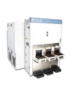 |
| The Applied Tetra Reticle Clean delivers damage-free, greater than 99% particle removal efficiency for 32nm and beyond photomasks, with the up to four times the throughput of any competitive system. (Photo: Business Wire) |
Abstract:
Applied Materials, Inc. today released its Applied Tetra™ Reticle Clean, the industry's only wet clean system that delivers damage-free, >99% particle removal efficiency for 32nm-and-beyond photomasks. Enabling customers to exceed 32nm specifications for critical mask cleaning applications, the compact Tetra Reticle Clean system also sets a new standard for productivity, offering up to four times the throughput of any competing system.
Applied Materials Sets the Standard for 32nm Mask Cleaning with New Tetra Reticle Clean System
TOKYO, Japan | Posted on April 15th, 2008 "Conventional photomask cleaning systems have not been able to meet the challenge of cleaning leading-edge masks effectively without damaging them," said Ajay Kumar, general manager of Applied Materials' Mask Etch and Cleans product division. "We've overcome this technology barrier with the Tetra Reticle Clean system, enabling mask makers to achieve the rapid cleaning performance they need while maintaining the mask feature integrity and phase control that their customers demand."
The Tetra Reticle Clean system's remarkable performance, which has already been validated in a 45nm production environment, is the result of several innovations in cleaning technology. The system features a unique, flexible design and sulfur-free, advanced ammonia-based cleaning agents that combine to maximize photoresist and particle removal without damaging the mask. Proprietary Uniform Cavitation Megasonics™ (UCM) technology distributes energy evenly over the entire mask surface, avoiding the damage-causing spikes generated by traditional point-source megasonic[1] cleans. The Tetra Reticle Clean system also introduces NanoDroplet™ technology which utilizes a unique nozzle design to create small, uniform, high-momentum droplets that evenly distribute energy and help deliver 32nm-and-beyond cleaning performance.
The benchmark high throughput of the Tetra Reticle Clean system is enabled by its ability to treat both sides of the mask simultaneously, cutting process time in half compared to other cleaning systems. This feature enables extendibility to future mask generations by allowing different chemistries to be used on each side without mixing. The system can be configured with multiple processing modules, offering mask makers the capacity to eliminate processing bottlenecks and reduce cycle times. For more information on the Applied Tetra Reticle Clean, visit www.appliedmaterials.com/products/reticle_clean_4.html.
The Tetra Reticle Clean system is part of Applied's expanding portfolio of photomask manufacturing and inspection solutions. The Applied Tetra Reticle Etch system is used by virtually every advanced mask shop in the world for 45nm photomask development and production. The Applied Aera2™ Mask Inspection system, just announced today, enables customers to immediately see what pattern will be printed on the wafer. These solutons will be showcased at the Applied Materials Technical Forum in Yokohama, Japan, on April 15 during SPIE Photomask Japan 2008. Visit www.appliedmaterials.com/2008_PMJ.
####
About Applied Materials, Inc.
Applied Materials, Inc. (Nasdaq:AMAT) is the global leader in Nanomanufacturing Technology™ solutions with a broad portfolio of innovative equipment, service and software products for the fabrication of semiconductor chips, flat panel displays, solar photovoltaic cells, flexible electronics and energy efficient glass. At Applied Materials, we apply Nanomanufacturing Technology to improve the way people live.
[1] Megasonic = the rapid formation and collapse of bubbles in a liquid caused by high-frequency pressure waves
For more information, please click here
Contacts:
Applied Materials, Inc.
Betty Newboe
408-563-0647 (editorial/media)
Linda Heller
408-986-7977 (financial community)
Copyright © Business Wire 2008
If you have a comment, please Contact us.Issuers of news releases, not 7th Wave, Inc. or Nanotechnology Now, are solely responsible for the accuracy of the content.
Bookmark:


| Related News Press |
News and information
![]() Quantum computer improves AI predictions April 17th, 2026
Quantum computer improves AI predictions April 17th, 2026
![]() Flexible sensor gains sensitivity under pressure April 17th, 2026
Flexible sensor gains sensitivity under pressure April 17th, 2026
![]() A reusable chip for particulate matter sensing April 17th, 2026
A reusable chip for particulate matter sensing April 17th, 2026
![]() Detecting vibrational quantum beating in the predissociation dynamics of SF6 using time-resolved photoelectron spectroscopy April 17th, 2026
Detecting vibrational quantum beating in the predissociation dynamics of SF6 using time-resolved photoelectron spectroscopy April 17th, 2026
Chip Technology
![]() A reusable chip for particulate matter sensing April 17th, 2026
A reusable chip for particulate matter sensing April 17th, 2026
![]() Metasurfaces smooth light to boost magnetic sensing precision January 30th, 2026
Metasurfaces smooth light to boost magnetic sensing precision January 30th, 2026
Announcements
![]() A fundamentally new therapeutic approach to cystic fibrosis: Nanobody repairs cellular defect April 17th, 2026
A fundamentally new therapeutic approach to cystic fibrosis: Nanobody repairs cellular defect April 17th, 2026
![]() UC Irvine physicists discover method to reverse ‘quantum scrambling’ : The work addresses the problem of information loss in quantum computing system April 17th, 2026
UC Irvine physicists discover method to reverse ‘quantum scrambling’ : The work addresses the problem of information loss in quantum computing system April 17th, 2026
Tools
![]() Metasurfaces smooth light to boost magnetic sensing precision January 30th, 2026
Metasurfaces smooth light to boost magnetic sensing precision January 30th, 2026
![]() From sensors to smart systems: the rise of AI-driven photonic noses January 30th, 2026
From sensors to smart systems: the rise of AI-driven photonic noses January 30th, 2026
![]() Japan launches fully domestically produced quantum computer: Expo visitors to experience quantum computing firsthand August 8th, 2025
Japan launches fully domestically produced quantum computer: Expo visitors to experience quantum computing firsthand August 8th, 2025
|
|
||
|
|
||
| The latest news from around the world, FREE | ||
|
|
||
|
|
||
| Premium Products | ||
|
|
||
|
Only the news you want to read!
Learn More |
||
|
|
||
|
Full-service, expert consulting
Learn More |
||
|
|
||