Home > Press > Mountbatten fractals inspired by nanotechnology
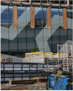 |
| Glass panels on the external wall of the clean room
Copyright: Sarah Prendergast |
Abstract:
The dynamic fractal patterns on the glass panels of the new Mountbatten Building were inspired by the School's research on optical nanotechnology.
Mountbatten fractals inspired by nanotechnology
Southampton, UK | Posted on December 10th, 2007In association with the Optoelectronics Research Centre, this research is being applied to create new optoelectronic devices which could enhance optical communications or greatly reduce the cost of solar energy.
The �55 million building, currently under construction and due for completion in July 2008, will provide a world-class facility that will allow the School of Electronics and Computer Science and the Optoelectronics Research Centre to make further contributions in these exciting areas of research.
The fractals, which form an ornamental design on the glass of the new building, are inspired by research into optical metamaterials, conducted by Dr Darren Bagnall and Dr Adrian Potts at the University's School of Electronics and Computer Science (ECS) working with Professor Nikolay Zheludev of the ORC.
�By drawing features that are much smaller than the wavelength of light, photons can be confused into doing things they normally wouldn't do,' said Dr Bagnall. �The chiral fractal structures when etched into glass at the nanoscale were shown to produce very unusual polarisation changes. By using similar technologies to produce other types of nanostructured arrays on the surfaces of solar cells we could also ensure that optical asymmetries are created that prevent light from escaping the solar cells.'
According to Dr Bagnall the light-trapping technologies could reduce the thickness of expensive semiconductor materials needed in solar panels, and this could directly reduce the cost of the devices. The first challenge is to prove that the technology works in practice, the second key challenge will be to develop cost-effective ways to produce nanopatterned layers.
The research will continue in the new Mountbatten Building. The state-of-the-art, interdisciplinary facility designed specifically to meet the long-term research needs of the School of Electronics and Computer Science and the Optoelectronics Research Centre, contains a large purpose-built clean room and associated laboratories, along with offices and meeting space.
'The technology which will be available in our new building, coupled with our high-quality academics, students and support staff, will enable us to develop faster, smaller, lower-cost, lower power, more environmentally-friendly devices for the next generations of electronic products whilst continuing our pioneering work in computer science,' said Professor Harvey Rutt, Head of ECS.
####
About University of Southampton
Southampton is already one of the top 10 research universities in the UK and has achieved consistently high scores for its teaching and learning activities.
We offer first-rate opportunities and facilities for study and research, and a stimulating working environment. Our strong enterprise agenda fosters close links with business and industry.
We currently have nearly 20,000 students and 5,000 staff based across several campuses in Southampton and Winchester. Our discipline base is broad, encompassing all the major academic subjects, but we also have a unique commitment to innovation, which is evidenced both in our outstanding research and scholarship at the leading edge, and also in our ability to pioneer new approaches and techniques relevant to the world today.
For more information, please click here
Contacts:
Research Contact:
Professor Nicholas Jennings
Tel: +44 (0)23 8059 7681
Copyright © University of Southampton
If you have a comment, please Contact us.Issuers of news releases, not 7th Wave, Inc. or Nanotechnology Now, are solely responsible for the accuracy of the content.
Bookmark:


| Related News Press |
Openings/New facilities/Groundbreaking/Expansion
![]() OCSiAl expands its graphene nanotube production capacities to Europe June 17th, 2022
OCSiAl expands its graphene nanotube production capacities to Europe June 17th, 2022
![]() GLOBALFOUNDRIES Moves Corporate Headquarters to its Most Advanced Semiconductor Manufacturing Facility in New York April 27th, 2021
GLOBALFOUNDRIES Moves Corporate Headquarters to its Most Advanced Semiconductor Manufacturing Facility in New York April 27th, 2021
![]() Oxford Instruments Plasma Technology relocates to advanced manufacturing facility: Move driven by exceptional business growth February 12th, 2021
Oxford Instruments Plasma Technology relocates to advanced manufacturing facility: Move driven by exceptional business growth February 12th, 2021
Announcements
![]() A fundamentally new therapeutic approach to cystic fibrosis: Nanobody repairs cellular defect April 17th, 2026
A fundamentally new therapeutic approach to cystic fibrosis: Nanobody repairs cellular defect April 17th, 2026
![]() UC Irvine physicists discover method to reverse �quantum scrambling� : The work addresses the problem of information loss in quantum computing system April 17th, 2026
UC Irvine physicists discover method to reverse �quantum scrambling� : The work addresses the problem of information loss in quantum computing system April 17th, 2026
Energy
![]() Sensors innovations for smart lithium-based batteries: advancements, opportunities, and potential challenges August 8th, 2025
Sensors innovations for smart lithium-based batteries: advancements, opportunities, and potential challenges August 8th, 2025
![]() Simple algorithm paired with standard imaging tool could predict failure in lithium metal batteries August 8th, 2025
Simple algorithm paired with standard imaging tool could predict failure in lithium metal batteries August 8th, 2025
Solar/Photovoltaic
![]() Spinel-type sulfide semiconductors to operate the next-generation LEDs and solar cells For solar-cell absorbers and green-LED source October 3rd, 2025
Spinel-type sulfide semiconductors to operate the next-generation LEDs and solar cells For solar-cell absorbers and green-LED source October 3rd, 2025
![]() KAIST researchers introduce new and improved, next-generation perovskite solar cell November 8th, 2024
KAIST researchers introduce new and improved, next-generation perovskite solar cell November 8th, 2024
![]() Groundbreaking precision in single-molecule optoelectronics August 16th, 2024
Groundbreaking precision in single-molecule optoelectronics August 16th, 2024
![]() Development of zinc oxide nanopagoda array photoelectrode: photoelectrochemical water-splitting hydrogen production January 12th, 2024
Development of zinc oxide nanopagoda array photoelectrode: photoelectrochemical water-splitting hydrogen production January 12th, 2024
|
|
||
|
|
||
| The latest news from around the world, FREE | ||
|
|
||
|
|
||
| Premium Products | ||
|
|
||
|
Only the news you want to read!
Learn More |
||
|
|
||
|
Full-service, expert consulting
Learn More |
||
|
|
||