Home > Press > Applied Materials Takes CMP Process Control to 45nm and Beyond With FullVision Endpoint System
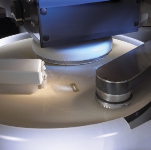 |
| The Applied FullVision CMP endpoint system is a major advancement over single wavelength endpoint technologies, offering twice the measurement accuracy with 50% higher reliability for dielectric applications, including oxide, STI and poly CMP. (Photo: Business Wire) |
Abstract:
Applied Materials, Inc. today announced its new Applied FullVision™ system that enables real-time control of dielectric CMP1 processes to the 45 nanometer (nm) device node and beyond. The FullVision system couples Applied's patented window-in-pad technology with multiple-wavelength spectroscopy to deliver advanced in situ endpoint capability for a variety of dielectric materials, including oxide, STI2, and poly CMP applications. The system demonstrates high repeatability across all applications with less than 150 angstrom, 3-sigma endpoint accuracy on patterned wafers. A major advance over single wavelength endpoint technologies, the FullVision system offers improved measurement accuracy with 50% higher reliability for dielectric applications.
Applied Materials Takes CMP Process Control to 45nm and Beyond With FullVision Endpoint System
SANTA CLARA, CA | Posted on November 29th, 2007 "CMP endpoint technology was pioneered by Applied Materials and is key to delivering benchmark CMP performance," said Dr. Hichem M'Saad, vice president and general manager of Applied Materials' Dielectric Systems and CMP Business Group. "As films become thinner, CMP becomes increasingly difficult, requiring much more precise wafer-to-wafer process control to achieve acceptable yields. Using broadband spectral analysis, FullVision technology monitors individual polishing zones across the wafer to provide twice the accuracy and repeatability of competitive systems on a wide variety of process steps - without compromising throughput. These are vital requirements for advanced device manufacturing."
The FullVision system has already been adopted by major memory customers on their Applied Reflexion® LK CMP systems in high volume manufacturing. For these customers, the system has enabled higher CMP yield by significantly reducing wafer scrap caused by drifts in consumable sets and incoming wafer profile variations.
Applied Materials leads the industry in CMP technology — with an installed base of more than 900 300mm CMP systems worldwide — and in providing advanced in situ metrology for ensuring best-of-breed planarization performance. See http://appliedmaterials.com/products/reflexion_lk_cmp_4.html for more information on the Applied FullVision endpoint system.
1 CMP=chemical mechanical planarization
2 STI=shallow trench isolation
####
About Applied Materials, Inc.
Applied Materials, Inc. (Nasdaq:AMAT) is the global leader in Nanomanufacturing Technology™ solutions with a broad portfolio of innovative equipment, service and software products for the fabrication of semiconductor chips, flat panel displays, solar photovoltaic cells, flexible electronics and energy efficient glass. At Applied Materials, we apply Nanomanufacturing Technology to improve the way people live.
For more information, please click here
Contacts:
Applied Materials, Inc.
Betty Newboe
408-563-0647 (editorial/media)
Randy Bane
408-986-7977 (financial community)
Copyright © Business Wire 2007
If you have a comment, please Contact us.Issuers of news releases, not 7th Wave, Inc. or Nanotechnology Now, are solely responsible for the accuracy of the content.
Bookmark:


| Related News Press |
Chip Technology
![]() A reusable chip for particulate matter sensing April 17th, 2026
A reusable chip for particulate matter sensing April 17th, 2026
![]() Metasurfaces smooth light to boost magnetic sensing precision January 30th, 2026
Metasurfaces smooth light to boost magnetic sensing precision January 30th, 2026
Announcements
![]() A fundamentally new therapeutic approach to cystic fibrosis: Nanobody repairs cellular defect April 17th, 2026
A fundamentally new therapeutic approach to cystic fibrosis: Nanobody repairs cellular defect April 17th, 2026
![]() UC Irvine physicists discover method to reverse ‘quantum scrambling’ : The work addresses the problem of information loss in quantum computing system April 17th, 2026
UC Irvine physicists discover method to reverse ‘quantum scrambling’ : The work addresses the problem of information loss in quantum computing system April 17th, 2026
Tools
![]() Metasurfaces smooth light to boost magnetic sensing precision January 30th, 2026
Metasurfaces smooth light to boost magnetic sensing precision January 30th, 2026
![]() From sensors to smart systems: the rise of AI-driven photonic noses January 30th, 2026
From sensors to smart systems: the rise of AI-driven photonic noses January 30th, 2026
![]() Japan launches fully domestically produced quantum computer: Expo visitors to experience quantum computing firsthand August 8th, 2025
Japan launches fully domestically produced quantum computer: Expo visitors to experience quantum computing firsthand August 8th, 2025
|
|
||
|
|
||
| The latest news from around the world, FREE | ||
|
|
||
|
|
||
| Premium Products | ||
|
|
||
|
Only the news you want to read!
Learn More |
||
|
|
||
|
Full-service, expert consulting
Learn More |
||
|
|
||