Home > Press > Placing single nanowires: NIST makes the connection
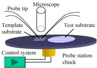 |
| Schematic of NIST single nanowire manipulation system. |
Abstract:
Researchers at the National Institute of Standards and Technology (NIST) have devised a system for manipulating and precisely positioning individual nanowires on semiconductor wafers. Their technique, described in a recent paper,* allows them to fabricate sophisticated test structures to explore the properties of nanowires, using only optical microscopy and conventional photolithographic processing in lieu of advanced (and expensive) tools such as focused ion or electron beams.
Placing single nanowires: NIST makes the connection
GAITHERSBURG, MD | Posted on April 27th, 2007Nanowires and nanotubes are being studied intensively as essential elements for future nanoscale electronics, but some fundamentals remain to be worked out�among them, how to put wires only a handful of atoms in diameter where you want them. The smallest-diameter nanowires today are built in a "bottom-up" fashion, assembled atom-by-atom through a chemical growth process such as chemical vapor deposition. This is essentially a bulk process; it produces haystacks of jumbled nanowires of varying lengths and diameters. "The normal research approach," explains NIST electronics engineer Curt Richter, "is to throw a whole bunch of these down on the test surface, hunt around with a microscope until you find a good-looking wire in about the right place, and use lithography to attach electrical contacts to it."
Scanning electron microscope image shows a single silicon nanowire positioned in an etched trench using NIST's nanowire manipulation technique. The trench helps keep the nanowire in position during the fabrication...
Click here for more information.
To achieve better control, the NIST engineers modified a standard probe station used to test individual components in microelectronic circuits. The station includes a high-resolution optical microscope and a system for precisely positioning work surfaces under a pair of customized titanium probes with tips less than 100 nanometers in diameter. In a two-step process, silicon nanowires suspended in a drop of water are deposited on a special staging wafer patterned with a grid of tiny posts, and dried. Resting on the tops of the posts, selected nanowires can be picked up by the two probe tips, which they cling to by static electricity. The test structure wafer is positioned under the probes, the nanowire is oriented by moving either the probe tips or the wafer, and then placed on the wafer in the desired position.
Although not at all suited to mass production, the technique's fine level of control allows NIST engineers to place single nanowires wherever they want to create elaborate structures for testing nanowire properties. They've demonstrated this by building a multiple-electrical-contact test structure for measuring the resistance of a nanowire independent of contact resistance, and a simple electromechanical "switch" suitable for measuring the flexibility of nanowires. They've used the technique successfully with nanowires greater than about 60 nm in diameter, and say sharper probe tips and high-resolution microscopes could push the limit lower.
*Q. Li, S. Koo, C.A. Richter, M.D. Edelstein, J.E. Bonevich, J.J. Kopanski, J.S. Suehle and E.M. Vogel. Precise alignment of single nanowires and fabrication of nanoelectromechanical switch and other test structures. IEEE Transactions on Nanotechnology. V.6, No.2. March 2007.
####
About National Institute of Standards and Technology (NIST)
From automated teller machines and atomic clocks to mammograms and semiconductors, innumerable products and services rely in some way on technology, measurement, and standards provided by the National Institute of Standards and Technology.
Founded in 1901, NIST is a non-regulatory federal agency within the U.S. Commerce Department's Technology Administration. NIST's mission is to promote U.S. innovation and industrial competitiveness by advancing measurement science, standards, and technology in ways that enhance economic security and improve our quality of life.
For more information, please click here
Contacts:
Michael Baum
301-975-2763
Copyright © National Institute of Standards and Technology (NIST)
If you have a comment, please Contact us.Issuers of news releases, not 7th Wave, Inc. or Nanotechnology Now, are solely responsible for the accuracy of the content.
Bookmark:


| Related News Press |
Nanotubes/Buckyballs/Fullerenes/Nanorods/Nanostrings/Nanosheets
![]() Tiny nanosheets, big leap: A new sensor detects ethanol at ultra-low levels January 30th, 2026
Tiny nanosheets, big leap: A new sensor detects ethanol at ultra-low levels January 30th, 2026
![]() Enhancing power factor of p- and n-type single-walled carbon nanotubes April 25th, 2025
Enhancing power factor of p- and n-type single-walled carbon nanotubes April 25th, 2025
![]() Chainmail-like material could be the future of armor: First 2D mechanically interlocked polymer exhibits exceptional flexibility and strength January 17th, 2025
Chainmail-like material could be the future of armor: First 2D mechanically interlocked polymer exhibits exceptional flexibility and strength January 17th, 2025
![]() Innovative biomimetic superhydrophobic coating combines repair and buffering properties for superior anti-erosion December 13th, 2024
Innovative biomimetic superhydrophobic coating combines repair and buffering properties for superior anti-erosion December 13th, 2024
Nanoelectronics
![]() Lab to industry: InSe wafer-scale breakthrough for future electronics August 8th, 2025
Lab to industry: InSe wafer-scale breakthrough for future electronics August 8th, 2025
![]() Interdisciplinary: Rice team tackles the future of semiconductors Multiferroics could be the key to ultralow-energy computing October 6th, 2023
Interdisciplinary: Rice team tackles the future of semiconductors Multiferroics could be the key to ultralow-energy computing October 6th, 2023
![]() Key element for a scalable quantum computer: Physicists from Forschungszentrum J�lich and RWTH Aachen University demonstrate electron transport on a quantum chip September 23rd, 2022
Key element for a scalable quantum computer: Physicists from Forschungszentrum J�lich and RWTH Aachen University demonstrate electron transport on a quantum chip September 23rd, 2022
![]() Reduced power consumption in semiconductor devices September 23rd, 2022
Reduced power consumption in semiconductor devices September 23rd, 2022
Discoveries
![]() Quantum computer improves AI predictions April 17th, 2026
Quantum computer improves AI predictions April 17th, 2026
![]() Flexible sensor gains sensitivity under pressure April 17th, 2026
Flexible sensor gains sensitivity under pressure April 17th, 2026
![]() A reusable chip for particulate matter sensing April 17th, 2026
A reusable chip for particulate matter sensing April 17th, 2026
![]() Detecting vibrational quantum beating in the predissociation dynamics of SF6 using time-resolved photoelectron spectroscopy April 17th, 2026
Detecting vibrational quantum beating in the predissociation dynamics of SF6 using time-resolved photoelectron spectroscopy April 17th, 2026
Announcements
![]() A fundamentally new therapeutic approach to cystic fibrosis: Nanobody repairs cellular defect April 17th, 2026
A fundamentally new therapeutic approach to cystic fibrosis: Nanobody repairs cellular defect April 17th, 2026
![]() UC Irvine physicists discover method to reverse �quantum scrambling� : The work addresses the problem of information loss in quantum computing system April 17th, 2026
UC Irvine physicists discover method to reverse �quantum scrambling� : The work addresses the problem of information loss in quantum computing system April 17th, 2026
|
|
||
|
|
||
| The latest news from around the world, FREE | ||
|
|
||
|
|
||
| Premium Products | ||
|
|
||
|
Only the news you want to read!
Learn More |
||
|
|
||
|
Full-service, expert consulting
Learn More |
||
|
|
||