Home > News > Old Company Press Releases > UWM News
Manufacturing Technique Offers Possibilities For Electronics Industry
Madison, WI. July 23rd, 2003
Manufacturing the minute may have gotten cheaper and more exact, thanks to a new technique developed by an international team of researchers.
The technique, described in the July 24 issue of the journal Nature, marries two approaches to lower the cost and improve the control of producing materials at the molecular level. This hybrid approach, say the researchers, could lead to computers, personal data assistants and cell phones that offer the densest data capacity stored in the tiniest packages.
About every 18 months, the number of transistors in computer chips doubles - the direct result of ever-shrinking sizes. By decreasing the size of these components and, consequently, fitting more of them onto a single chip, computer speed and power improves, explains Paul Nealey, a University of Wisconsin-Madison chemical engineer and senior author of the paper.
For this trend to continue, as most experts expect it will during the next 20 years, science, technology and the techniques used to produce microelectronics - for example, the transistors inside integrated circuits - will need to operate on an even smaller scale, says Nealey.
"Where the electronics industry is going is the manufacturing of devices that have ever-decreasing dimensions," says the engineer, adding that the goal is to take the scale down from around 130 nanometers to under 50 nanometers (a nanometer equals one billionth of a meter).
But achieving these nanoscale dimensions - and the speedy, powerful products that could result - is hindered by limitations in the standard manufacturing method used to develop the tiny devices inside computer chips. The approach, which uses a process called lithography to build the different layers that make up microelectronic devices, currently is cost-prohibitive at a smaller scale, says Nealey.
Another approach that could be used to build smaller microelectronic devices exists, but it has its own set of limitations. The method relies on long chains of molecules called block copolymers that arrange themselves into patterns on a given surface.
"With self-assembling materials, achieving dimensions of tens of nanometers is inexpensive and routine," says Nealey. But, he adds, although the method may be cheap, it can result in defects and does not meet the numerous constraints of fabrication.
By merging the principles of both techniques, researchers at UW-Madison and the Paul Scherrer Institute in Switzerland developed a hybrid approach that maximizes the benefits and minimizes the limitations of each technique.
"Our emphasis is on combining the approaches, using the desirable attributes of both, to get molecular-level control in the existing manufacturing processes," Nealey explains.
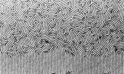
Specifically, the team of researchers used lithography to create patterns in the surface chemistry of a polymeric material. Then, they deposited a film of block copolymers on the surface, where the molecules arranged themselves into the underlying pattern without imperfections.
"Tremendous promise exists for the development of hybrid technologies such as this one in which self-assembling materials are integrated into existing manufacturing processes to deliver nanoscale control and meet exacting fabrication constraints," says Nealey.
The most promising application for such a hybrid technology, he adds, could be the development of magnetic storage media with nearly the maximum possible capacity per unit area. In addition, this new technology could lead to the design of new microelectronic devices with unknown potential.
The new work was conducted at the Center for NanoTechnology at UW-Madison's Synchrotron Radiation Center. It was funded in part by National Science Foundation's Materials Research Science and Engineering Center and the Semiconductor Research Corporation, a consortium that sponsors university research worldwide.
Contact: Paul Nealey
(608) 265-8171
nealey@engr.wisc.edu
Reprinted with premission. Copyright UWM.
If you have a comment, please
us.
|
|
||
|
|
||
| The latest news from around the world, FREE | ||
|
|
||
|
|
||
| Premium Products | ||
|
|
||
|
Only the news you want to read!
Learn More |
||
|
|
||
|
Full-service, expert consulting
Learn More |
||
|
|
||
