Home > Press > Transparent graphene electrodes might lead to new generation of solar cells: New roll-to-roll production method could enable lightweight, flexible solar devices and a new generation of display screens
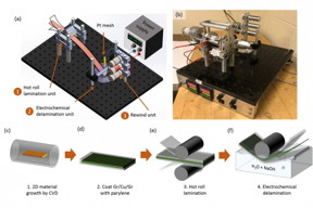 |
| A new manufacturing process for graphene is based on using an intermediate carrier layer of material after the graphene is laid down through a vapor deposition process. The carrier allows the ultrathin graphene sheet, less than a nanometer (billionth of a meter) thick, to be easily lifted off from a substrate, allowing for rapid roll-to-roll manufacturing. These figures show this process for making graphene sheets, along with a photo of the proof-of-concept device used (b). Courtesy of the researchers |
Abstract:
A new way of making large sheets of high-quality, atomically thin graphene could lead to ultra-lightweight, flexible solar cells, and to new classes of light-emitting devices and other thin-film electronics.
Transparent graphene electrodes might lead to new generation of solar cells: New roll-to-roll production method could enable lightweight, flexible solar devices and a new generation of display screens
Cambridge, MA | Posted on June 8th, 2020The new manufacturing process, which was developed at MIT and should be relatively easy to scale up for industrial production, involves an intermediate �buffer� layer of material that is key to the technique�s success. The buffer allows the ultrathin graphene sheet, less than a nanometer (billionth of a meter) thick, to be easily lifted off from its substrate, allowing for rapid roll-to-roll manufacturing.
The process is detailed in a paper published yesterday in Advanced Functional Materials, by MIT postdocs Giovanni Azzellino and Mahdi Tavakoli; professors Jing Kong, Tomas Palacios, and Markus Buehler; and five others at MIT.
Finding a way to make thin, large-area, transparent electrodes that are stable in open air has been a major quest in thin-film electronics in recent years, for a variety of applications in optoelectronic devices � things that either emit light, like computer and smartphone screens, or harvest it, like solar cells. Today�s standard for such applications is indium tin oxide (ITO), a material based on rare and expensive chemical elements.
Many research groups have worked on finding a replacement for ITO, focusing on both organic and inorganic candidate materials. Graphene, a form of pure carbon whose atoms are arranged in a flat hexagonal array, has extremely good electrical and mechanical properties, yet it is vanishingly thin, physically flexible, and made from an abundant, inexpensive material. Furthermore, it can be easily grown in the form of large sheets by chemical vapor deposition (CVD), using copper as a seed layer, as Kong�s group has demonstrated. However, for device applications, the trickiest part has been finding ways to release the CVD-grown graphene from its native copper substrate.
This release, known as graphene transfer process, tends to result in a web of tears, wrinkles, and defects in the sheets, which disrupts the film continuity and therefore drastically reduces their electrical conductivity. But with the new technology, Azzellino says, �now we are able to reliably manufacture large-area graphene sheets, transfer them onto whatever substrate we want, and the way we transfer them does not affect the electrical and mechanical properties of the pristine graphene.�
The key is the buffer layer, made of a polymer material called parylene, that conforms at the atomic level to the graphene sheets on which it is deployed. Like graphene, parylene is produced by CVD, which simplifies the manufacturing process and scalability.
As a demonstration of this technology, the team made proof-of-concept solar cells, adopting a thin-film polymeric solar cell material, along with the newly formed graphene layer for one of the cell�s two electrodes, and a parylene layer that also serves as a device substrate. They measured an optical transmittance close to 90 percent for the graphene film under visible light.
The prototyped graphene-based solar cell improves by roughly 36 times the delivered power per weight, compared to ITO-based state-of-the-art devices. It also uses 1/200 the amount of material per unit area for the transparent electrode. And, there is a further fundamental advantage compared to ITO: �Graphene comes for almost free,� Azzellino says.
�Ultra-lightweight graphene-based devices can pave the way to a new generation of applications,� he says. �So if you think about portable devices, the power per weight becomes a very important figure of merit. What if we could deploy a transparent solar cell on your tablet that is able to power up the tablet itself?� Though some further development would be needed, such applications should ultimately be feasible with this new method, he says.
The buffer material, parylene, is widely used in the microelectronics industry, usually to encapsulate and protect electronic devices. So the supply chains and equipment for using the material already are widespread, Azzellino says. Of the three existing types of parylene, the team�s tests showed that one of them, which contains more chlorine atoms, was by far the most effective for this application.
The atomic proximity of chlorine-rich parylene to the underlying graphene as the layers are sandwiched together provides a further advantage, by offering a kind of �doping� for graphene, finally providing a more reliable and nondestructive approach for conductivity improvement of large-area graphene, unlike many others that have been tested and reported so far.
�The graphene and the parylene films are always face-to-face,� Azzellino says. �So basically, the doping action is always there, and therefore the advantage is permanent.�
The research team also included Marek Hempel, Ang-Yu Lu, Francisco Martin-Martinez, Jiayuan Zhao and Jingjie Yeo, all at MIT. The work was supported by Eni SpA through the MIT Energy Initiative, the U.S. Army Research Office through the Institute for Soldier Nanotechnologies, and the Office of Naval Research.
####
For more information, please click here
Contacts:
Abby Abazorius
Phone: 617-253-2709
MIT News Office
Copyright © Massachusetts Institute of Technology
If you have a comment, please Contact us.Issuers of news releases, not 7th Wave, Inc. or Nanotechnology Now, are solely responsible for the accuracy of the content.
Bookmark:


| Related News Press |
News and information
![]() Quantum computer improves AI predictions April 17th, 2026
Quantum computer improves AI predictions April 17th, 2026
![]() Flexible sensor gains sensitivity under pressure April 17th, 2026
Flexible sensor gains sensitivity under pressure April 17th, 2026
![]() A reusable chip for particulate matter sensing April 17th, 2026
A reusable chip for particulate matter sensing April 17th, 2026
![]() Detecting vibrational quantum beating in the predissociation dynamics of SF6 using time-resolved photoelectron spectroscopy April 17th, 2026
Detecting vibrational quantum beating in the predissociation dynamics of SF6 using time-resolved photoelectron spectroscopy April 17th, 2026
2 Dimensional Materials
![]() Flexible sensor gains sensitivity under pressure April 17th, 2026
Flexible sensor gains sensitivity under pressure April 17th, 2026
![]() MXene nanomaterials enter a new dimension Multilayer nanomaterial: MXene flakes created at Drexel University show new promise as 1D scrolls January 30th, 2026
MXene nanomaterials enter a new dimension Multilayer nanomaterial: MXene flakes created at Drexel University show new promise as 1D scrolls January 30th, 2026
![]() ICFO researchers overcome long-standing bottleneck in single photon detection with twisted 2D materials August 8th, 2025
ICFO researchers overcome long-standing bottleneck in single photon detection with twisted 2D materials August 8th, 2025
![]() First real-time observation of two-dimensional melting process: Researchers at Mainz University unveil new insights into magnetic vortex structures August 8th, 2025
First real-time observation of two-dimensional melting process: Researchers at Mainz University unveil new insights into magnetic vortex structures August 8th, 2025
![]() Lab to industry: InSe wafer-scale breakthrough for future electronics August 8th, 2025
Lab to industry: InSe wafer-scale breakthrough for future electronics August 8th, 2025
Thin films
![]() Tiny nanosheets, big leap: A new sensor detects ethanol at ultra-low levels January 30th, 2026
Tiny nanosheets, big leap: A new sensor detects ethanol at ultra-low levels January 30th, 2026
Display technology/LEDs/SS Lighting/OLEDs
![]() Spinel-type sulfide semiconductors to operate the next-generation LEDs and solar cells For solar-cell absorbers and green-LED source October 3rd, 2025
Spinel-type sulfide semiconductors to operate the next-generation LEDs and solar cells For solar-cell absorbers and green-LED source October 3rd, 2025
Graphene/ Graphite
![]() Electrifying results shed light on graphene foam as a potential material for lab grown cartilage June 6th, 2025
Electrifying results shed light on graphene foam as a potential material for lab grown cartilage June 6th, 2025
![]() Breakthrough in proton barrier films using pore-free graphene oxide: Kumamoto University researchers achieve new milestone in advanced coating technologies September 13th, 2024
Breakthrough in proton barrier films using pore-free graphene oxide: Kumamoto University researchers achieve new milestone in advanced coating technologies September 13th, 2024
Govt.-Legislation/Regulation/Funding/Policy
![]() Quantum computer improves AI predictions April 17th, 2026
Quantum computer improves AI predictions April 17th, 2026
![]() Metasurfaces smooth light to boost magnetic sensing precision January 30th, 2026
Metasurfaces smooth light to boost magnetic sensing precision January 30th, 2026
![]() New imaging approach transforms study of bacterial biofilms August 8th, 2025
New imaging approach transforms study of bacterial biofilms August 8th, 2025
Possible Futures
![]() A fundamentally new therapeutic approach to cystic fibrosis: Nanobody repairs cellular defect April 17th, 2026
A fundamentally new therapeutic approach to cystic fibrosis: Nanobody repairs cellular defect April 17th, 2026
![]() UC Irvine physicists discover method to reverse �quantum scrambling� : The work addresses the problem of information loss in quantum computing system April 17th, 2026
UC Irvine physicists discover method to reverse �quantum scrambling� : The work addresses the problem of information loss in quantum computing system April 17th, 2026
Discoveries
![]() Quantum computer improves AI predictions April 17th, 2026
Quantum computer improves AI predictions April 17th, 2026
![]() Flexible sensor gains sensitivity under pressure April 17th, 2026
Flexible sensor gains sensitivity under pressure April 17th, 2026
![]() A reusable chip for particulate matter sensing April 17th, 2026
A reusable chip for particulate matter sensing April 17th, 2026
![]() Detecting vibrational quantum beating in the predissociation dynamics of SF6 using time-resolved photoelectron spectroscopy April 17th, 2026
Detecting vibrational quantum beating in the predissociation dynamics of SF6 using time-resolved photoelectron spectroscopy April 17th, 2026
Materials/Metamaterials/Magnetoresistance
![]() First real-time observation of two-dimensional melting process: Researchers at Mainz University unveil new insights into magnetic vortex structures August 8th, 2025
First real-time observation of two-dimensional melting process: Researchers at Mainz University unveil new insights into magnetic vortex structures August 8th, 2025
![]() Researchers unveil a groundbreaking clay-based solution to capture carbon dioxide and combat climate change June 6th, 2025
Researchers unveil a groundbreaking clay-based solution to capture carbon dioxide and combat climate change June 6th, 2025
![]() A 1960s idea inspires NBI researchers to study hitherto inaccessible quantum states June 6th, 2025
A 1960s idea inspires NBI researchers to study hitherto inaccessible quantum states June 6th, 2025
![]() Institute for Nanoscience hosts annual proposal planning meeting May 16th, 2025
Institute for Nanoscience hosts annual proposal planning meeting May 16th, 2025
Announcements
![]() A fundamentally new therapeutic approach to cystic fibrosis: Nanobody repairs cellular defect April 17th, 2026
A fundamentally new therapeutic approach to cystic fibrosis: Nanobody repairs cellular defect April 17th, 2026
![]() UC Irvine physicists discover method to reverse �quantum scrambling� : The work addresses the problem of information loss in quantum computing system April 17th, 2026
UC Irvine physicists discover method to reverse �quantum scrambling� : The work addresses the problem of information loss in quantum computing system April 17th, 2026
Interviews/Book Reviews/Essays/Reports/Podcasts/Journals/White papers/Posters
![]() A fundamentally new therapeutic approach to cystic fibrosis: Nanobody repairs cellular defect April 17th, 2026
A fundamentally new therapeutic approach to cystic fibrosis: Nanobody repairs cellular defect April 17th, 2026
![]() UC Irvine physicists discover method to reverse �quantum scrambling� : The work addresses the problem of information loss in quantum computing system April 17th, 2026
UC Irvine physicists discover method to reverse �quantum scrambling� : The work addresses the problem of information loss in quantum computing system April 17th, 2026
Military
![]() Quantum engineers �squeeze� laser frequency combs to make more sensitive gas sensors January 17th, 2025
Quantum engineers �squeeze� laser frequency combs to make more sensitive gas sensors January 17th, 2025
![]() Chainmail-like material could be the future of armor: First 2D mechanically interlocked polymer exhibits exceptional flexibility and strength January 17th, 2025
Chainmail-like material could be the future of armor: First 2D mechanically interlocked polymer exhibits exceptional flexibility and strength January 17th, 2025
![]() Single atoms show their true color July 5th, 2024
Single atoms show their true color July 5th, 2024
![]() NRL charters Navy�s quantum inertial navigation path to reduce drift April 5th, 2024
NRL charters Navy�s quantum inertial navigation path to reduce drift April 5th, 2024
Energy
![]() Sensors innovations for smart lithium-based batteries: advancements, opportunities, and potential challenges August 8th, 2025
Sensors innovations for smart lithium-based batteries: advancements, opportunities, and potential challenges August 8th, 2025
![]() Simple algorithm paired with standard imaging tool could predict failure in lithium metal batteries August 8th, 2025
Simple algorithm paired with standard imaging tool could predict failure in lithium metal batteries August 8th, 2025
Photonics/Optics/Lasers
![]() Metasurfaces smooth light to boost magnetic sensing precision January 30th, 2026
Metasurfaces smooth light to boost magnetic sensing precision January 30th, 2026
![]() From sensors to smart systems: the rise of AI-driven photonic noses January 30th, 2026
From sensors to smart systems: the rise of AI-driven photonic noses January 30th, 2026
Solar/Photovoltaic
![]() Spinel-type sulfide semiconductors to operate the next-generation LEDs and solar cells For solar-cell absorbers and green-LED source October 3rd, 2025
Spinel-type sulfide semiconductors to operate the next-generation LEDs and solar cells For solar-cell absorbers and green-LED source October 3rd, 2025
![]() KAIST researchers introduce new and improved, next-generation perovskite solar cell November 8th, 2024
KAIST researchers introduce new and improved, next-generation perovskite solar cell November 8th, 2024
![]() Groundbreaking precision in single-molecule optoelectronics August 16th, 2024
Groundbreaking precision in single-molecule optoelectronics August 16th, 2024
![]() Development of zinc oxide nanopagoda array photoelectrode: photoelectrochemical water-splitting hydrogen production January 12th, 2024
Development of zinc oxide nanopagoda array photoelectrode: photoelectrochemical water-splitting hydrogen production January 12th, 2024
|
|
||
|
|
||
| The latest news from around the world, FREE | ||
|
|
||
|
|
||
| Premium Products | ||
|
|
||
|
Only the news you want to read!
Learn More |
||
|
|
||
|
Full-service, expert consulting
Learn More |
||
|
|
||