Home > Press > JEOL Introduces New Field Emission SEM With Automated Analytical Intelligence
 |
Abstract:
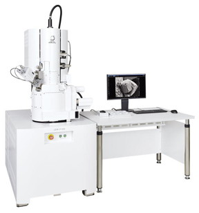
JEOL introduces a new Field Emission Scanning Electron Microscope with several features unique to the company’s FE SEM product line: NeoEngine, employing analytical intelligence for optimizing electron beam setup and tuning; embedded EDS with Live Analysis for real time imaging and elemental analysis; and Zeromag navigation function, seamlessly transitioning between optical imaging to nanoscale investigation with the high-powered optics of the SEM.
JEOL Introduces New Field Emission SEM With Automated Analytical Intelligence
Peabody, MA | Posted on January 29th, 2020"JEOL’s F100 FE-SEM offers a truly revolutionary approach to address users’ high-resolution microscopy and microanalysis needs. In a single platform JEOL combined the best electron optics with fully embedded EDS microanalysis and the powerful AI algorithms of NeoEngine to achieve the ultimate ease of use and streamlined workflow," says Dr. Natasha Erdman, FESEM Product Manager.
NeoEngine corrects electron trajectories and automatically aligns the beam in real time, plus automatically corrects focus, brightness/contrast, and astigmatism. The SEM achieves single-digit Angstrom resolution at low kV, ideal for ultrahigh high-resolution imaging of nanostructures, specimen surface details, biological specimens, and magnetic samples as well as elemental analysis of non-conductive and beam sensitive samples.
Fully embedded EDS with Live Analysis allows the user to simply select the area, mapping, line, or another type of analysis directly on the observation screen to begin automatic live display of the elements in the specified location.
The large specimen chamber of the JSM-F100 features multiple ports for analytical applications: EDS, WDS, EBSD, STEM, BSE, and CL. An optional Soft X-ray Emission Spectrometer provides efficient and parallel collection of very low-energy X-rays while providing unprecedented chemical state analysis.
The JEOL JSM-F100 features an in-lens detector and energy filter, an Aperture Angle Control Lens (ACL) for superb resolution at any kV or probe current, Beam Deceleration (BD) mode for charge reduction and enhanced surface detail, and a variable pressure option for non-conductive specimens.
Never before has the power of Field Emission SEM been so easy to use. With the introduction of JEOL’s next-generation streamlined FE SEM product line, operator controls are simplified and the functions of the SEM fully automated for optimum performance. Imaging and analysis data are quickly obtained and reported through the effortless data management system.
Further information: www.jeolusa.com/PRODUCTS/Scanning-Electron-Microscopes-SEM/FE-SEM
The JEOL SEM can be configured with detectors that make it essentially a nanolab in addition to the high resolution imaging of samples.
Here’s an explanation of the acronyms for the analytical techniques mentioned in the text that can be done with the JEOL microscope depending on what information the user needs to extract from the sample.
EDS Energy Dispersive X-Ray Spectroscopy (detects X-Rays from the sample)
WDS Wavelength Dispersive Spectroscopy (for quantitative measurements)
EBSD Electron Backscatter Diffraction (for crystal orientation)
STEM Scanning Transmission Electron Microscopy
BSE Backscattered Electron Imaging
CL Cathodoluminescence (for luminescent materials)
####
For more information, please click here
Contacts:
11 Dearborn Road | Peabody, MA 01930
978-536-2309
Copyright © JEOL USA
If you have a comment, please Contact us.Issuers of news releases, not 7th Wave, Inc. or Nanotechnology Now, are solely responsible for the accuracy of the content.
| Related News Press |
News and information
![]() Quantum computer improves AI predictions April 17th, 2026
Quantum computer improves AI predictions April 17th, 2026
![]() Flexible sensor gains sensitivity under pressure April 17th, 2026
Flexible sensor gains sensitivity under pressure April 17th, 2026
![]() A reusable chip for particulate matter sensing April 17th, 2026
A reusable chip for particulate matter sensing April 17th, 2026
![]() Detecting vibrational quantum beating in the predissociation dynamics of SF6 using time-resolved photoelectron spectroscopy April 17th, 2026
Detecting vibrational quantum beating in the predissociation dynamics of SF6 using time-resolved photoelectron spectroscopy April 17th, 2026
Imaging
![]() Simple algorithm paired with standard imaging tool could predict failure in lithium metal batteries August 8th, 2025
Simple algorithm paired with standard imaging tool could predict failure in lithium metal batteries August 8th, 2025
Announcements
![]() A fundamentally new therapeutic approach to cystic fibrosis: Nanobody repairs cellular defect April 17th, 2026
A fundamentally new therapeutic approach to cystic fibrosis: Nanobody repairs cellular defect April 17th, 2026
![]() UC Irvine physicists discover method to reverse ‘quantum scrambling’ : The work addresses the problem of information loss in quantum computing system April 17th, 2026
UC Irvine physicists discover method to reverse ‘quantum scrambling’ : The work addresses the problem of information loss in quantum computing system April 17th, 2026
Tools
![]() Metasurfaces smooth light to boost magnetic sensing precision January 30th, 2026
Metasurfaces smooth light to boost magnetic sensing precision January 30th, 2026
![]() From sensors to smart systems: the rise of AI-driven photonic noses January 30th, 2026
From sensors to smart systems: the rise of AI-driven photonic noses January 30th, 2026
![]() Japan launches fully domestically produced quantum computer: Expo visitors to experience quantum computing firsthand August 8th, 2025
Japan launches fully domestically produced quantum computer: Expo visitors to experience quantum computing firsthand August 8th, 2025
|
|
||
|
|
||
| The latest news from around the world, FREE | ||
|
|
||
|
|
||
| Premium Products | ||
|
|
||
|
Only the news you want to read!
Learn More |
||
|
|
||
|
Full-service, expert consulting
Learn More |
||
|
|
||


