Home > Press > Can't get thinner than this: synthesis of atomically flat boron sheets
 |
Abstract:
Scientists at Tokyo Institute of Technology (Tokyo Tech) find a simple method for producing atomically thin layers of oxidized borophene, a promising 2D boron-based nanomaterial that could serve in a variety of fields.
Can't get thinner than this: synthesis of atomically flat boron sheets
Tokyo, Japan | Posted on August 23rd, 2019Since its rediscovery and characterization in 2004, graphene has been the focus of countless research efforts across multiple fields. It is a very versatile material consisting of a two-dimensional (2D) carbon network; in other words, it comprises a thin sheet of carbon that has a thickness of one atom. Graphene is not only stronger than the strongest steels, but also has a myriad of interesting chemical, electronic, and mechanical characteristics that has left scientists wondering if similar 2D networks of other materials could have such useful properties.
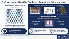
One novel 2D material that was recently reported is borophene, an analogue of graphene but consisting of boron atoms instead of carbon atoms. However, as one would expect for 2D sheets of any material, the synthesis of borophene has proved to be challenging. Researchers either require the use of a substrate to make borophene more stable or coupling boron with hydroxyl groups (OH-), which causes the structure to not be atomically flat.
In a recent study conducted at Tokyo Institute of Technology, a research team including Tetsuya Kambe, Akiyoshi Kuzume and Kimihisa Yamamoto was successful in synthesizing atomically flat oxidized borophene sheets through a simple solution-based method. First, they synthesized stacked layers of borophene oxide through a fairly simple process using a potassium borohydride salt (KBH4). An X-ray analysis revealed the 2D-layered structure of the material, in which layers of boron atoms forming a hexagonal 2D network with oxygen atoms as bridges were intercalated with layers containing potassium atoms. Then, the subsequent necessary step was to find a way to exfoliate atomically thin layers of the borophene oxide network. The researchers achieved this by putting the material in dimethylformamide, which is a commonly used organic solvent. Various types of measurements were carried out to verify the structure of the exfoliated sheets, including electron microscopy, spectroscopy, and atomic force microscopy. The results confirmed that the proposed method was effective for producing the desired atomically flat oxidized borophene sheets.
Finally, the researchers performed resistivity measurements to analyze the conducting properties of stacked borophene sheets and found an interesting characteristic referred to as anisotropy. This means that the sheets exhibited different types of conductivity depending on the direction of the current flow. The material behaved like a semiconductor in the inter-plane direction, whereas it exhibited metal-like behavior in the in-plane direction of the boron network. The mechanisms behind these two types of conducting behaviors were elucidated as well. "It is important to note that our boron sheets can be handled easily at ambient conditions," remarks Dr. Kambe, indicating that this pioneering research could be the basis for finding potential applications for borophene.
Finding facile methods for the synthesis of borophene and borophene-based compounds is crucial to conducting further research on this interesting material and its potential uses. "Like graphene, borophene is expected to have unique properties, including extraordinary mechanical characteristics and metallic behavior that could be exploited in a variety of fields," states Dr. Kambe. Hopefully, future findings and developments on 2D materials will enable us to employ their exotic properties and tailor them to suit our needs.
####
For more information, please click here
Contacts:
Assistant Professor Tetsuya Kambe
Institute of Innovative Research
Email
Tel +81-45-924-5259
Contact
Public Relations Section, Tokyo Institute of Technology
Email
Tel +81-3-5734-2975
Copyright © Tokyo Institute of Technology
If you have a comment, please Contact us.Issuers of news releases, not 7th Wave, Inc. or Nanotechnology Now, are solely responsible for the accuracy of the content.
Bookmark:


| Related Links |
| Related News Press |
News and information
![]() Quantum computer improves AI predictions April 17th, 2026
Quantum computer improves AI predictions April 17th, 2026
![]() Flexible sensor gains sensitivity under pressure April 17th, 2026
Flexible sensor gains sensitivity under pressure April 17th, 2026
![]() A reusable chip for particulate matter sensing April 17th, 2026
A reusable chip for particulate matter sensing April 17th, 2026
![]() Detecting vibrational quantum beating in the predissociation dynamics of SF6 using time-resolved photoelectron spectroscopy April 17th, 2026
Detecting vibrational quantum beating in the predissociation dynamics of SF6 using time-resolved photoelectron spectroscopy April 17th, 2026
2 Dimensional Materials
![]() Flexible sensor gains sensitivity under pressure April 17th, 2026
Flexible sensor gains sensitivity under pressure April 17th, 2026
![]() MXene nanomaterials enter a new dimension Multilayer nanomaterial: MXene flakes created at Drexel University show new promise as 1D scrolls January 30th, 2026
MXene nanomaterials enter a new dimension Multilayer nanomaterial: MXene flakes created at Drexel University show new promise as 1D scrolls January 30th, 2026
![]() ICFO researchers overcome long-standing bottleneck in single photon detection with twisted 2D materials August 8th, 2025
ICFO researchers overcome long-standing bottleneck in single photon detection with twisted 2D materials August 8th, 2025
![]() First real-time observation of two-dimensional melting process: Researchers at Mainz University unveil new insights into magnetic vortex structures August 8th, 2025
First real-time observation of two-dimensional melting process: Researchers at Mainz University unveil new insights into magnetic vortex structures August 8th, 2025
Thin films
![]() Tiny nanosheets, big leap: A new sensor detects ethanol at ultra-low levels January 30th, 2026
Tiny nanosheets, big leap: A new sensor detects ethanol at ultra-low levels January 30th, 2026
Graphene/ Graphite
![]() Electrifying results shed light on graphene foam as a potential material for lab grown cartilage June 6th, 2025
Electrifying results shed light on graphene foam as a potential material for lab grown cartilage June 6th, 2025
![]() Breakthrough in proton barrier films using pore-free graphene oxide: Kumamoto University researchers achieve new milestone in advanced coating technologies September 13th, 2024
Breakthrough in proton barrier films using pore-free graphene oxide: Kumamoto University researchers achieve new milestone in advanced coating technologies September 13th, 2024
Possible Futures
![]() A fundamentally new therapeutic approach to cystic fibrosis: Nanobody repairs cellular defect April 17th, 2026
A fundamentally new therapeutic approach to cystic fibrosis: Nanobody repairs cellular defect April 17th, 2026
![]() UC Irvine physicists discover method to reverse �quantum scrambling� : The work addresses the problem of information loss in quantum computing system April 17th, 2026
UC Irvine physicists discover method to reverse �quantum scrambling� : The work addresses the problem of information loss in quantum computing system April 17th, 2026
Discoveries
![]() Quantum computer improves AI predictions April 17th, 2026
Quantum computer improves AI predictions April 17th, 2026
![]() Flexible sensor gains sensitivity under pressure April 17th, 2026
Flexible sensor gains sensitivity under pressure April 17th, 2026
![]() A reusable chip for particulate matter sensing April 17th, 2026
A reusable chip for particulate matter sensing April 17th, 2026
![]() Detecting vibrational quantum beating in the predissociation dynamics of SF6 using time-resolved photoelectron spectroscopy April 17th, 2026
Detecting vibrational quantum beating in the predissociation dynamics of SF6 using time-resolved photoelectron spectroscopy April 17th, 2026
Materials/Metamaterials/Magnetoresistance
![]() First real-time observation of two-dimensional melting process: Researchers at Mainz University unveil new insights into magnetic vortex structures August 8th, 2025
First real-time observation of two-dimensional melting process: Researchers at Mainz University unveil new insights into magnetic vortex structures August 8th, 2025
![]() Researchers unveil a groundbreaking clay-based solution to capture carbon dioxide and combat climate change June 6th, 2025
Researchers unveil a groundbreaking clay-based solution to capture carbon dioxide and combat climate change June 6th, 2025
![]() A 1960s idea inspires NBI researchers to study hitherto inaccessible quantum states June 6th, 2025
A 1960s idea inspires NBI researchers to study hitherto inaccessible quantum states June 6th, 2025
![]() Institute for Nanoscience hosts annual proposal planning meeting May 16th, 2025
Institute for Nanoscience hosts annual proposal planning meeting May 16th, 2025
Announcements
![]() A fundamentally new therapeutic approach to cystic fibrosis: Nanobody repairs cellular defect April 17th, 2026
A fundamentally new therapeutic approach to cystic fibrosis: Nanobody repairs cellular defect April 17th, 2026
![]() UC Irvine physicists discover method to reverse �quantum scrambling� : The work addresses the problem of information loss in quantum computing system April 17th, 2026
UC Irvine physicists discover method to reverse �quantum scrambling� : The work addresses the problem of information loss in quantum computing system April 17th, 2026
Interviews/Book Reviews/Essays/Reports/Podcasts/Journals/White papers/Posters
![]() A fundamentally new therapeutic approach to cystic fibrosis: Nanobody repairs cellular defect April 17th, 2026
A fundamentally new therapeutic approach to cystic fibrosis: Nanobody repairs cellular defect April 17th, 2026
![]() UC Irvine physicists discover method to reverse �quantum scrambling� : The work addresses the problem of information loss in quantum computing system April 17th, 2026
UC Irvine physicists discover method to reverse �quantum scrambling� : The work addresses the problem of information loss in quantum computing system April 17th, 2026
|
|
||
|
|
||
| The latest news from around the world, FREE | ||
|
|
||
|
|
||
| Premium Products | ||
|
|
||
|
Only the news you want to read!
Learn More |
||
|
|
||
|
Full-service, expert consulting
Learn More |
||
|
|
||