Home > Press > Atomically thin light-emitting device opens the possibility for 'invisible' displays
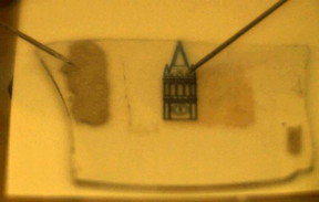 |
| Gif of the device in action. Probes inject positive and negative charges in the light emitting device, which is transparent under the campanile outline, producing bright light. CREDIT Javey lab. |
Abstract:
UC Berkeley engineers have built a bright-light emitting device that is millimeters wide and fully transparent when turned off. The light emitting material in this device is a monolayer semiconductor, which is just three atoms thick.
Atomically thin light-emitting device opens the possibility for 'invisible' displays
Berkeley, CA | Posted on March 26th, 2018The device opens the door to invisible displays on walls and windows - displays that would be bright when turned on but see-through when turned off -- or in futuristic applications such as light-emitting tattoos, according to the researchers.
"The materials are so thin and flexible that the device can be made transparent and can conform to curved surfaces," said Der-Hsien Lien, a postdoctoral fellow at UC Berkeley and a co-first author along with Matin Amani and Sujay Desai, both doctoral students in the Department of Electrical Engineering and Computer Sciences at Berkeley.
Their study was published March 26 in the journal Nature Communications. The work was funded by the National Science Foundation and the Department of Energy.
The device was developed in the laboratory of Ali Javey, professor of Electrical Engineering and Computer Sciences at Berkeley. In 2015, Javey's lab published research in the journal Science showing that monolayer semiconductors are capable of emitting bright light, but stopped short of building a light-emitting device. The new work in Nature Communications overcame fundamental barriers in utilizing LED technology on monolayer semiconductors, allowing for such devices to be scaled from sizes smaller than the width of a human hair up to several millimeters. That means that researchers can keep the thickness small, but make the lateral dimensions (width and length) large, so that the light intensity can be high.
Commercial LEDs consist of a semiconductor material that is electrically injected with positive and negative charges, which produce light when they meet. Typically, two contact points are used in a semiconductor-based light emitting device; one for injecting negatively charged particles and one injecting positively charged particles. Making contacts that can efficiently inject these charges is a fundamental challenge for LEDs, and it is particularly challenging for monolayer semiconductors since there is so little material to work with.
The Berkeley research team engineered a way to circumvent this challenge by designing a new device that only requires one contact on the semiconductor. By laying the semiconductor monolayer on an insulator and placing electrodes on the monolayer and underneath the insulator, the researchers could apply an AC signal across the insulator. During the moment when the AC signal switches its polarity from positive to negative (and vice versa), both positive and negative charges are present at the same time in the semiconductor, creating light.
The researchers showed that this mechanism works in four different monolayer materials, all of which emit different colors of light.
This device is a proof-of-concept, and much research still remains, primarily to improve efficiency. Measuring this device's efficiency is not straightforward, but the researchers think it's about 1 percent efficient. Commercial LEDs have efficiencies of around 25 to 30 percent.
The concept may be applicable to other devices and other kinds of materials, the device could one day have applications in a number of fields where having invisible displays are warranted. That could be an atomically thin display that's imprinted on a wall or even on human skin.
"A lot of work remains to be done and a number of challenges need to be overcome to further advance the technology for practical applications," Javey said. "However, this is one step forward by presenting a device architecture for easy injection of both charges into monolayer semiconductors."
####
For more information, please click here
Contacts:
Brett Israel
510-643-7741
Copyright © University of California, Berkeley
If you have a comment, please Contact us.Issuers of news releases, not 7th Wave, Inc. or Nanotechnology Now, are solely responsible for the accuracy of the content.
Bookmark:


| Related News Press |
News and information
![]() Quantum computer improves AI predictions April 17th, 2026
Quantum computer improves AI predictions April 17th, 2026
![]() Flexible sensor gains sensitivity under pressure April 17th, 2026
Flexible sensor gains sensitivity under pressure April 17th, 2026
![]() A reusable chip for particulate matter sensing April 17th, 2026
A reusable chip for particulate matter sensing April 17th, 2026
![]() Detecting vibrational quantum beating in the predissociation dynamics of SF6 using time-resolved photoelectron spectroscopy April 17th, 2026
Detecting vibrational quantum beating in the predissociation dynamics of SF6 using time-resolved photoelectron spectroscopy April 17th, 2026
2 Dimensional Materials
![]() Flexible sensor gains sensitivity under pressure April 17th, 2026
Flexible sensor gains sensitivity under pressure April 17th, 2026
![]() ICFO researchers overcome long-standing bottleneck in single photon detection with twisted 2D materials August 8th, 2025
ICFO researchers overcome long-standing bottleneck in single photon detection with twisted 2D materials August 8th, 2025
![]() First real-time observation of two-dimensional melting process: Researchers at Mainz University unveil new insights into magnetic vortex structures August 8th, 2025
First real-time observation of two-dimensional melting process: Researchers at Mainz University unveil new insights into magnetic vortex structures August 8th, 2025
![]() Lab to industry: InSe wafer-scale breakthrough for future electronics August 8th, 2025
Lab to industry: InSe wafer-scale breakthrough for future electronics August 8th, 2025
Display technology/LEDs/SS Lighting/OLEDs
![]() Spinel-type sulfide semiconductors to operate the next-generation LEDs and solar cells For solar-cell absorbers and green-LED source October 3rd, 2025
Spinel-type sulfide semiconductors to operate the next-generation LEDs and solar cells For solar-cell absorbers and green-LED source October 3rd, 2025
Govt.-Legislation/Regulation/Funding/Policy
![]() Quantum computer improves AI predictions April 17th, 2026
Quantum computer improves AI predictions April 17th, 2026
![]() Metasurfaces smooth light to boost magnetic sensing precision January 30th, 2026
Metasurfaces smooth light to boost magnetic sensing precision January 30th, 2026
![]() New imaging approach transforms study of bacterial biofilms August 8th, 2025
New imaging approach transforms study of bacterial biofilms August 8th, 2025
Possible Futures
![]() A fundamentally new therapeutic approach to cystic fibrosis: Nanobody repairs cellular defect April 17th, 2026
A fundamentally new therapeutic approach to cystic fibrosis: Nanobody repairs cellular defect April 17th, 2026
![]() UC Irvine physicists discover method to reverse �quantum scrambling� : The work addresses the problem of information loss in quantum computing system April 17th, 2026
UC Irvine physicists discover method to reverse �quantum scrambling� : The work addresses the problem of information loss in quantum computing system April 17th, 2026
Discoveries
![]() Quantum computer improves AI predictions April 17th, 2026
Quantum computer improves AI predictions April 17th, 2026
![]() Flexible sensor gains sensitivity under pressure April 17th, 2026
Flexible sensor gains sensitivity under pressure April 17th, 2026
![]() A reusable chip for particulate matter sensing April 17th, 2026
A reusable chip for particulate matter sensing April 17th, 2026
![]() Detecting vibrational quantum beating in the predissociation dynamics of SF6 using time-resolved photoelectron spectroscopy April 17th, 2026
Detecting vibrational quantum beating in the predissociation dynamics of SF6 using time-resolved photoelectron spectroscopy April 17th, 2026
Materials/Metamaterials/Magnetoresistance
![]() First real-time observation of two-dimensional melting process: Researchers at Mainz University unveil new insights into magnetic vortex structures August 8th, 2025
First real-time observation of two-dimensional melting process: Researchers at Mainz University unveil new insights into magnetic vortex structures August 8th, 2025
![]() Researchers unveil a groundbreaking clay-based solution to capture carbon dioxide and combat climate change June 6th, 2025
Researchers unveil a groundbreaking clay-based solution to capture carbon dioxide and combat climate change June 6th, 2025
![]() A 1960s idea inspires NBI researchers to study hitherto inaccessible quantum states June 6th, 2025
A 1960s idea inspires NBI researchers to study hitherto inaccessible quantum states June 6th, 2025
![]() Institute for Nanoscience hosts annual proposal planning meeting May 16th, 2025
Institute for Nanoscience hosts annual proposal planning meeting May 16th, 2025
Announcements
![]() A fundamentally new therapeutic approach to cystic fibrosis: Nanobody repairs cellular defect April 17th, 2026
A fundamentally new therapeutic approach to cystic fibrosis: Nanobody repairs cellular defect April 17th, 2026
![]() UC Irvine physicists discover method to reverse �quantum scrambling� : The work addresses the problem of information loss in quantum computing system April 17th, 2026
UC Irvine physicists discover method to reverse �quantum scrambling� : The work addresses the problem of information loss in quantum computing system April 17th, 2026
Interviews/Book Reviews/Essays/Reports/Podcasts/Journals/White papers/Posters
![]() A fundamentally new therapeutic approach to cystic fibrosis: Nanobody repairs cellular defect April 17th, 2026
A fundamentally new therapeutic approach to cystic fibrosis: Nanobody repairs cellular defect April 17th, 2026
![]() UC Irvine physicists discover method to reverse �quantum scrambling� : The work addresses the problem of information loss in quantum computing system April 17th, 2026
UC Irvine physicists discover method to reverse �quantum scrambling� : The work addresses the problem of information loss in quantum computing system April 17th, 2026
|
|
||
|
|
||
| The latest news from around the world, FREE | ||
|
|
||
|
|
||
| Premium Products | ||
|
|
||
|
Only the news you want to read!
Learn More |
||
|
|
||
|
Full-service, expert consulting
Learn More |
||
|
|
||