Home > Press > Department of Materials Test Engineering (WPT) at TU Dortmund University uses Deben CT5000TEC stage to perform X-ray micro-tomography experiments for better understanding of damage progression in composite materials
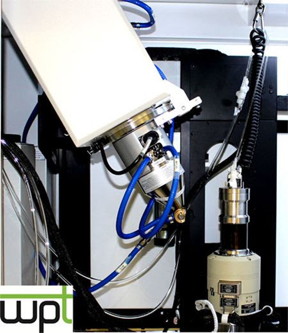 |
| The CT5000TEC (Deben) mounted in a X TH 160 device (Nikon). |
Abstract:
Deben, a leading provider of in situ testing stages together with innovative accessories and components for electron microscopy, reports on how TU Dortmund University is using their CT5000TEC compression/tensile stage to study fiber-reinforced composites. This work is being performed using a Nikon X-ray source
Department of Materials Test Engineering (WPT) at TU Dortmund University uses Deben CT5000TEC stage to perform X-ray micro-tomography experiments for better understanding of damage progression in composite materials
Woolpit, UK | Posted on March 13th, 2018Ronja Scholz is a scientific assistant and PhD student in the group of Prof. Dr. Frank Walther, Head of the Department of Materials Test Engineering (WPT) at TU Dortmund University. She specialises in the use of computed tomography (CT) to characterise composite materials contributing to the scientific and industrial research projects. These deal with investigations concerning metals, additively manufactured materials and composites using modern measurement and inspection processes, supported by optimized analysis and evaluation techniques. WPT provides the database for construction and production as well as for virtual development of reliable high-performance products for different industries and is used for decision-making guidance for material selection, quality control, component monitoring and damage analysis. This is facilitated by determining the chemical composition, analyzing microstructural properties with light, electron beams and X-rays, determining material properties and characteristic values by means of destructive (DT) and non-destructive testing (NDT) methods.
Ms. Scholz describes her work applying CT. �Our investigations provide microstructural information of a material as a non-destructive testing technique. The ability to look inside a specimen or component and getting 3D volume information, which can be characterized concerning different structural issues like defect volume, fiber orientation or wall thickness, expanded the test technology of our department in a very efficient way. Thus, to really understand the interdependencies between microstructure, mechanical loading and climatic implied processes in materials as accurate as possible, in situ investigations are of great importance. Therefore, the use of the Deben's CT5000TEC stage in combination with Nikon XT H 160 kV microfocus X-ray source enables the capture of the current state of a material in situ under mechanical tensile or compression loads up to 5 kN and variable temperatures in the range of -20 �C to +160 �C, see Figure 1. These measurements give essential information about defects such as pores or delaminations in the material�s initial condition as well as the progression and development of these defects under mechanical loading. This strategy allows the evaluation of different process routes for the manufacturing of a material allowing the study of the resulting microstructure as well as the performance of the material or component under application-oriented conditions such as elevated temperatures. When comparing CT scans of a damaged composite specimen, the in situ scan results reveal significantly more damage than the results of a conventionally performed scan. Figure 2a visualizes the damage development in a fiber-reinforced plastic. This material shows great potential as a substitute material for metals in automotive and aero applications providing economic efficiency thanks to their high specific strength. To gather sufficient information about the load capacity, damage development and the use of composites under changing environmental conditions, detailed investigations are necessary. In Figure 2b, the development of the defect volume due to increasing tensile load is shown for a cellulose-based composite, which shall be utilized as resource-efficient construction material. These results generated at room temperature can now be correlated with investigations at elevated or degraded temperatures, depending on the area of application.�
�Lastly, it is important to note that before using the integrable Deben CT5000TEC stage, we focused on conventional CT investigations, where specimens are scanned while resting (no load applied) to characterize their specific structure, e.g. fiber orientation, pore content, wall thicknesses, etc. Now our experiments produce data that is much realistic to the in-life use of these exciting, new composite materials.�
To obtain full details of the Deben applications and product portfolio, please visit www.deben.co.uk.
References
Tenkamp, J.; Koch, A.; Knorre, S.; Krupp, U.; Michels, W.; Walther, F.: Defect-correlated fatigue assessment of A356-T6 aluminum cast alloy using computed tomography based Kitagawa-Takahashi diagrams. International Journal of Fatigue 108 (2018) 25-34.
Goerlich, P.; Scholz, R.; Walther, F.: Micro-CT defect analysis and hardness distribution of flat-face extruded EN AW606 aluminium chips. Materials Testing 59, 7-8 (2017) 613-617.
Siddique, S.; Imran, M.; Rauer, M.; Kaloudis, M.; Wycisk, E.; Emmelmann, C.; Walther, F.: Computed tomography for characterization of fatigue performance of selective laser melted parts. Materials & Design 83 (2015) 661-669.
A collective list of the publications can be reviewed under: http://wpt.mb.tu-dortmund.de/cms/de/forschung/publikationen/index.php
####
About Deben
Deben are a UK precision engineering company specialising in the field of in-situ tensile testing, motion control and specimen cooling for microscopy applications. Established in 1986 and named after a Suffolk river, Deben now operate from a large, modern business unit in Woolpit near Bury St. Edmunds in Suffolk. The product groups are motor control systems, in-situ micro-tensile stages, Peltier heating & cooling stages, detectors for SEMs and electro-static beam blankers. The company also makes custom and OEM versions of these products to specifically meet customer requirements.
Deben provide consultancy, design and prototype manufacturing services. In house facilities include SolidWorks and SolidEdge 3D CAD and COSMOS finite element analysis software, CNC machining, electronics design and manufacture and software design using Visual C++, Microsoft.net and DirectX. Utilising these resources and experience, Deben manufacture products for OEMs and end users in the UK and overseas.
Deben UK Ltd. is a subsidiary company of UK based Judges Scientific plc. For details on Deben and all its products & solutions, visit www.deben.co.uk.
About WPT
All information about the Department of Materials Test Engineering (WPT) at TU Dortmund University are available under www.wpt-info.de
For more information, please click here
Contacts:
Deben UK Limited
Brickfields Business Park
Old Stowmarket Road
Woolpit, Bury St Edmunds
Suffolk IP30 9QS, UK
T +44 (0)1359 244870
www.deben.co.uk
Talking Science Limited
39 de Bohun Court
Saffron Walden
Essex CB10 2BA
T +44(0)1799 521881
M +44(0)7843 012997
www.talking-science.com
Copyright © Deben
If you have a comment, please Contact us.Issuers of news releases, not 7th Wave, Inc. or Nanotechnology Now, are solely responsible for the accuracy of the content.
Bookmark:


| Related News Press |
News and information
![]() Quantum computer improves AI predictions April 17th, 2026
Quantum computer improves AI predictions April 17th, 2026
![]() Flexible sensor gains sensitivity under pressure April 17th, 2026
Flexible sensor gains sensitivity under pressure April 17th, 2026
![]() A reusable chip for particulate matter sensing April 17th, 2026
A reusable chip for particulate matter sensing April 17th, 2026
![]() Detecting vibrational quantum beating in the predissociation dynamics of SF6 using time-resolved photoelectron spectroscopy April 17th, 2026
Detecting vibrational quantum beating in the predissociation dynamics of SF6 using time-resolved photoelectron spectroscopy April 17th, 2026
Imaging
![]() Simple algorithm paired with standard imaging tool could predict failure in lithium metal batteries August 8th, 2025
Simple algorithm paired with standard imaging tool could predict failure in lithium metal batteries August 8th, 2025
Nanomedicine
![]() A fundamentally new therapeutic approach to cystic fibrosis: Nanobody repairs cellular defect April 17th, 2026
A fundamentally new therapeutic approach to cystic fibrosis: Nanobody repairs cellular defect April 17th, 2026
![]() New molecular technology targets tumors and simultaneously silences two �undruggable� cancer genes August 8th, 2025
New molecular technology targets tumors and simultaneously silences two �undruggable� cancer genes August 8th, 2025
![]() New imaging approach transforms study of bacterial biofilms August 8th, 2025
New imaging approach transforms study of bacterial biofilms August 8th, 2025
![]() Electrifying results shed light on graphene foam as a potential material for lab grown cartilage June 6th, 2025
Electrifying results shed light on graphene foam as a potential material for lab grown cartilage June 6th, 2025
Announcements
![]() A fundamentally new therapeutic approach to cystic fibrosis: Nanobody repairs cellular defect April 17th, 2026
A fundamentally new therapeutic approach to cystic fibrosis: Nanobody repairs cellular defect April 17th, 2026
![]() UC Irvine physicists discover method to reverse �quantum scrambling� : The work addresses the problem of information loss in quantum computing system April 17th, 2026
UC Irvine physicists discover method to reverse �quantum scrambling� : The work addresses the problem of information loss in quantum computing system April 17th, 2026
Interviews/Book Reviews/Essays/Reports/Podcasts/Journals/White papers/Posters
![]() A fundamentally new therapeutic approach to cystic fibrosis: Nanobody repairs cellular defect April 17th, 2026
A fundamentally new therapeutic approach to cystic fibrosis: Nanobody repairs cellular defect April 17th, 2026
![]() UC Irvine physicists discover method to reverse �quantum scrambling� : The work addresses the problem of information loss in quantum computing system April 17th, 2026
UC Irvine physicists discover method to reverse �quantum scrambling� : The work addresses the problem of information loss in quantum computing system April 17th, 2026
Tools
![]() Metasurfaces smooth light to boost magnetic sensing precision January 30th, 2026
Metasurfaces smooth light to boost magnetic sensing precision January 30th, 2026
![]() From sensors to smart systems: the rise of AI-driven photonic noses January 30th, 2026
From sensors to smart systems: the rise of AI-driven photonic noses January 30th, 2026
![]() Japan launches fully domestically produced quantum computer: Expo visitors to experience quantum computing firsthand August 8th, 2025
Japan launches fully domestically produced quantum computer: Expo visitors to experience quantum computing firsthand August 8th, 2025
Nanobiotechnology
![]() A fundamentally new therapeutic approach to cystic fibrosis: Nanobody repairs cellular defect April 17th, 2026
A fundamentally new therapeutic approach to cystic fibrosis: Nanobody repairs cellular defect April 17th, 2026
![]() New molecular technology targets tumors and simultaneously silences two �undruggable� cancer genes August 8th, 2025
New molecular technology targets tumors and simultaneously silences two �undruggable� cancer genes August 8th, 2025
![]() New imaging approach transforms study of bacterial biofilms August 8th, 2025
New imaging approach transforms study of bacterial biofilms August 8th, 2025
![]() Electrifying results shed light on graphene foam as a potential material for lab grown cartilage June 6th, 2025
Electrifying results shed light on graphene foam as a potential material for lab grown cartilage June 6th, 2025
|
|
||
|
|
||
| The latest news from around the world, FREE | ||
|
|
||
|
|
||
| Premium Products | ||
|
|
||
|
Only the news you want to read!
Learn More |
||
|
|
||
|
Full-service, expert consulting
Learn More |
||
|
|
||