Home > Press > MEMS chips get metatlenses: Combining metasurface lenses with MEMS technology could add high-speed scanning and enhance focusing capability of optical systems
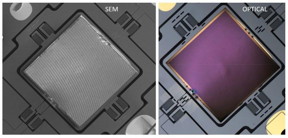 |
| Metasurface-based flat lens integrated onto a MEMS scanner: Scanning electron micrograph (left) and optical microscope image (right) of a lens-on-MEMS device. Integration of MEMS devices with metalenses will help to create a new paradigm to manipulate light by combining the strength of these technologies: high-speed dynamic control with precise spatial manipulation of wave-fronts. CREDIT Center for Nanoscale Materials, Argonne National Lab |
Abstract:
Lens technologies have advanced across all scales, from digital cameras and high bandwidth in fiber optics to the LIGO lab instruments. Now, a new lens technology that could be produced using standard computer-chip technology is emerging and could replace the bulky layers and complex geometries of traditional curved lenses.
MEMS chips get metatlenses: Combining metasurface lenses with MEMS technology could add high-speed scanning and enhance focusing capability of optical systems
Washington, DC | Posted on February 21st, 2018Flat lenses, unlike their traditional counterparts, are relatively lightweight, based on optical nanomaterials known as metasurfaces. When the subwavelength nanostructures of a metasurface form certain repeated patterns, they mimic the complex curvatures that refract light, but with less bulk and an improved ability to focus light with reduced distortion. However, most of these nanostructured devices are static, which limits their functionality.
Federico Capasso, an applied physicist at Harvard University who pioneered metalens technology, and Daniel Lopez, group leader of nanofabrication and devices at Argonne National Laboratory and an early developer of microelectromechanical systems (MEMS), brainstormed about adding motion capabilities like fast scanning and beam steering to metalenses for new applications.
Capasso and Lopez developed a device that integrates mid-infrared spectrum metalenses onto MEMS. The researchers report their findings this week in APL Photonics, from AIP Publishing.
MEMS is a circuit-based technology that incorporates microelectronics, like those found in computer chips, and includes mechanical microstructures like actuators and gears. Ubiquitous in everything from cellphones to airbags, biosensing devices, appliances and optics, MEMS are fabricated using the same techniques used for integrated circuits on typical computer chips.
"Dense integration of thousands of individually controlled lens-on-MEMS devices onto a single silicon chip would allow an unprecedented degree of control and manipulation of the optical field," Lopez Said.
The researchers formed the metasurface lens using standard photolithography techniques on a silicon-on-insulator wafer with a 2-micron-thick top device layer, a 200-nanometer buried-oxide layer, and a 600-micron-thick handle layer. Then, they placed the flat lens onto a MEMS scanner, essentially a micromirror that deflects light for high-speed optical path length modulation. They aligned the lens with the MEMS' central platform and fixed them together by depositing small platinum patches.
"Our MEMS-integrated metasurface lens prototype can be electrically controlled to vary the angular rotation of a flat lens and can scan the focal spot by several degrees," Lopez said. "Furthermore, this proof-of-concept integration of metasurface-based flat lenses with MEMS scanners can be extended to the visible and other parts of the electromagnetic spectrum, implying the potential for application across wider fields, such as MEMS-based microscope systems, holographic and projection imaging, LIDAR (light detection and ranging) scanners and laser printing."
When electrostatically actuated, the MEMS platform controls the angle of the lens along two orthogonal axes, allowing the scanning of the flat lens focal spot by about 9 degrees in each direction. The researchers estimate that the focusing efficiency is about 85 percent.
"Such metalenses can be mass produced with the same computer-chip fabrication technology and in the future, will replace conventional lenses in a wide range of applications," Capasso said.
####
About American Institute of Physics
APL Photonics is the dedicated home for open access multidisciplinary research from and for the photonics community. The journal publishes fundamental and applied results that significantly advance the knowledge in photonics across physics, chemistry, biology and materials science. See http://aip.scitation.org/journal/app .
For more information, please click here
Contacts:
Julia Majors
301-209-3090
Copyright © American Institute of Physics
If you have a comment, please Contact us.Issuers of news releases, not 7th Wave, Inc. or Nanotechnology Now, are solely responsible for the accuracy of the content.
Bookmark:


| Related Links |
| Related News Press |
News and information
![]() Quantum computer improves AI predictions April 17th, 2026
Quantum computer improves AI predictions April 17th, 2026
![]() Flexible sensor gains sensitivity under pressure April 17th, 2026
Flexible sensor gains sensitivity under pressure April 17th, 2026
![]() A reusable chip for particulate matter sensing April 17th, 2026
A reusable chip for particulate matter sensing April 17th, 2026
![]() Detecting vibrational quantum beating in the predissociation dynamics of SF6 using time-resolved photoelectron spectroscopy April 17th, 2026
Detecting vibrational quantum beating in the predissociation dynamics of SF6 using time-resolved photoelectron spectroscopy April 17th, 2026
Imaging
![]() Simple algorithm paired with standard imaging tool could predict failure in lithium metal batteries August 8th, 2025
Simple algorithm paired with standard imaging tool could predict failure in lithium metal batteries August 8th, 2025
Possible Futures
![]() A fundamentally new therapeutic approach to cystic fibrosis: Nanobody repairs cellular defect April 17th, 2026
A fundamentally new therapeutic approach to cystic fibrosis: Nanobody repairs cellular defect April 17th, 2026
![]() UC Irvine physicists discover method to reverse �quantum scrambling� : The work addresses the problem of information loss in quantum computing system April 17th, 2026
UC Irvine physicists discover method to reverse �quantum scrambling� : The work addresses the problem of information loss in quantum computing system April 17th, 2026
MEMS
Discoveries
![]() Quantum computer improves AI predictions April 17th, 2026
Quantum computer improves AI predictions April 17th, 2026
![]() Flexible sensor gains sensitivity under pressure April 17th, 2026
Flexible sensor gains sensitivity under pressure April 17th, 2026
![]() A reusable chip for particulate matter sensing April 17th, 2026
A reusable chip for particulate matter sensing April 17th, 2026
![]() Detecting vibrational quantum beating in the predissociation dynamics of SF6 using time-resolved photoelectron spectroscopy April 17th, 2026
Detecting vibrational quantum beating in the predissociation dynamics of SF6 using time-resolved photoelectron spectroscopy April 17th, 2026
Announcements
![]() A fundamentally new therapeutic approach to cystic fibrosis: Nanobody repairs cellular defect April 17th, 2026
A fundamentally new therapeutic approach to cystic fibrosis: Nanobody repairs cellular defect April 17th, 2026
![]() UC Irvine physicists discover method to reverse �quantum scrambling� : The work addresses the problem of information loss in quantum computing system April 17th, 2026
UC Irvine physicists discover method to reverse �quantum scrambling� : The work addresses the problem of information loss in quantum computing system April 17th, 2026
Interviews/Book Reviews/Essays/Reports/Podcasts/Journals/White papers/Posters
![]() A fundamentally new therapeutic approach to cystic fibrosis: Nanobody repairs cellular defect April 17th, 2026
A fundamentally new therapeutic approach to cystic fibrosis: Nanobody repairs cellular defect April 17th, 2026
![]() UC Irvine physicists discover method to reverse �quantum scrambling� : The work addresses the problem of information loss in quantum computing system April 17th, 2026
UC Irvine physicists discover method to reverse �quantum scrambling� : The work addresses the problem of information loss in quantum computing system April 17th, 2026
Tools
![]() Metasurfaces smooth light to boost magnetic sensing precision January 30th, 2026
Metasurfaces smooth light to boost magnetic sensing precision January 30th, 2026
![]() From sensors to smart systems: the rise of AI-driven photonic noses January 30th, 2026
From sensors to smart systems: the rise of AI-driven photonic noses January 30th, 2026
![]() Japan launches fully domestically produced quantum computer: Expo visitors to experience quantum computing firsthand August 8th, 2025
Japan launches fully domestically produced quantum computer: Expo visitors to experience quantum computing firsthand August 8th, 2025
|
|
||
|
|
||
| The latest news from around the world, FREE | ||
|
|
||
|
|
||
| Premium Products | ||
|
|
||
|
Only the news you want to read!
Learn More |
||
|
|
||
|
Full-service, expert consulting
Learn More |
||
|
|
||