Home > Press > Engineers shrink microscope to dime-sized device
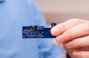 |
| A MEMS-based atomic force microscope developed by engineers at the University of Texas at Dallas is about 1 square centimeter in size (top center). Here it is attached to a small printed circuit board that contains circuitry, sensors and other miniaturized components that control the movement and other aspects of the device. CREDIT University of Texas at Dallas |
Abstract:
Researchers at The University of Texas at Dallas have created an atomic force microscope on a chip, dramatically shrinking the size -- and, hopefully, the price tag -- of a high-tech device commonly used to characterize material properties.
Engineers shrink microscope to dime-sized device
Dallas, TX | Posted on February 17th, 2017"A standard atomic force microscope is a large, bulky instrument, with multiple control loops, electronics and amplifiers," said Dr. Reza Moheimani, professor of mechanical engineering at UT Dallas. "We have managed to miniaturize all of the electromechanical components down onto a single small chip."
Moheimani and his colleagues describe their prototype device in this month's issue of the IEEE Journal of Microelectromechanical Systems.
An atomic force microscope (AFM) is a scientific tool that is used to create detailed three-dimensional images of the surfaces of materials, down to the nanometer scale -- that's roughly on the scale of individual molecules.
The basic AFM design consists of a tiny cantilever, or arm, that has a sharp tip attached to one end. As the apparatus scans back and forth across the surface of a sample, or the sample moves under it, the interactive forces between the sample and the tip cause the cantilever to move up and down as the tip follows the contours of the surface. Those movements are then translated into an image.
"An AFM is a microscope that 'sees' a surface kind of the way a visually impaired person might, by touching. You can get a resolution that is well beyond what an optical microscope can achieve," said Moheimani, who holds the James Von Ehr Distinguished Chair in Science and Technology in the Erik Jonsson School of Engineering and Computer Science. "It can capture features that are very, very small."
The UT Dallas team created its prototype on-chip AFM using a microelectromechanical systems (MEMS) approach.
"A classic example of MEMS technology are the accelerometers and gyroscopes found in smartphones," said Dr. Anthony Fowler, a research scientist in Moheimani's Laboratory for Dynamics and Control of Nanosystems and one of the article's co-authors. "These used to be big, expensive, mechanical devices, but using MEMS technology, accelerometers have shrunk down onto a single chip, which can be manufactured for just a few dollars apiece."
The MEMS-based AFM is about 1 square centimeter in size, or a little smaller than a dime. It is attached to a small printed circuit board, about half the size of a credit card, which contains circuitry, sensors and other miniaturized components that control the movement and other aspects of the device.
Conventional AFMs operate in various modes. Some map out a sample's features by maintaining a constant force as the probe tip drags across the surface, while others do so by maintaining a constant distance between the two. "The problem with using a constant height approach is that the tip is applying varying forces on a sample all the time, which can damage a sample that is very soft," Fowler said. "Or, if you are scanning a very hard surface, you could wear down the tip,"
The MEMS-based AFM operates in "tapping mode," which means the cantilever and tip oscillate up and down perpendicular to the sample, and the tip alternately contacts then lifts off from the surface. As the probe moves back and forth across a sample material, a feedback loop maintains the height of that oscillation, ultimately creating an image.
"In tapping mode, as the oscillating cantilever moves across the surface topography, the amplitude of the oscillation wants to change as it interacts with sample," said Dr. Mohammad Maroufi, a research associate in mechanical engineering and co-author of the paper. "This device creates an image by maintaining the amplitude of oscillation."
Because conventional AFMs require lasers and other large components to operate, their use can be limited. They're also expensive.
"An educational version can cost about $30,000 or $40,000, and a laboratory-level AFM can run $500,000 or more," Moheimani said. "Our MEMS approach to AFM design has the potential to significantly reduce the complexity and cost of the instrument.
"One of the attractive aspects about MEMS is that you can mass produce them, building hundreds or thousands of them in one shot, so the price of each chip would only be a few dollars. As a result, you might be able to offer the whole miniature AFM system for a few thousand dollars."
A reduced size and price tag also could expand the AFMs' utility beyond current scientific applications.
"For example, the semiconductor industry might benefit from these small devices, in particular companies that manufacture the silicon wafers from which computer chips are made," Moheimani said. "With our technology, you might have an array of AFMs to characterize the wafer's surface to find micro-faults before the product is shipped out." The lab prototype is a first-generation device, Moheimani said, and the group is already working on ways to improve and streamline the fabrication of the device.
"This is one of those technologies where, as they say, 'If you build it, they will come.' We anticipate finding many applications as the technology matures," Moheimani said.
###
In addition to the UT Dallas researchers, Michael Ruppert, a visiting graduate student from the University of Newcastle in Australia, was a co-author of the journal article. Moheimani was Ruppert's doctoral advisor.
Moheimani's research has been funded by UT Dallas startup funds, the Von Ehr Distinguished Chair and the Defense Advanced Research Projects Agency.
####
For more information, please click here
Contacts:
Amanda Siegfried
972-883-4335
Copyright © University of Texas at Dallas
If you have a comment, please Contact us.Issuers of news releases, not 7th Wave, Inc. or Nanotechnology Now, are solely responsible for the accuracy of the content.
Bookmark:


| Related Links |
| Related News Press |
News and information
![]() Quantum computer improves AI predictions April 17th, 2026
Quantum computer improves AI predictions April 17th, 2026
![]() Flexible sensor gains sensitivity under pressure April 17th, 2026
Flexible sensor gains sensitivity under pressure April 17th, 2026
![]() A reusable chip for particulate matter sensing April 17th, 2026
A reusable chip for particulate matter sensing April 17th, 2026
![]() Detecting vibrational quantum beating in the predissociation dynamics of SF6 using time-resolved photoelectron spectroscopy April 17th, 2026
Detecting vibrational quantum beating in the predissociation dynamics of SF6 using time-resolved photoelectron spectroscopy April 17th, 2026
Imaging
![]() Simple algorithm paired with standard imaging tool could predict failure in lithium metal batteries August 8th, 2025
Simple algorithm paired with standard imaging tool could predict failure in lithium metal batteries August 8th, 2025
Govt.-Legislation/Regulation/Funding/Policy
![]() Quantum computer improves AI predictions April 17th, 2026
Quantum computer improves AI predictions April 17th, 2026
![]() Metasurfaces smooth light to boost magnetic sensing precision January 30th, 2026
Metasurfaces smooth light to boost magnetic sensing precision January 30th, 2026
![]() New imaging approach transforms study of bacterial biofilms August 8th, 2025
New imaging approach transforms study of bacterial biofilms August 8th, 2025
Possible Futures
![]() A fundamentally new therapeutic approach to cystic fibrosis: Nanobody repairs cellular defect April 17th, 2026
A fundamentally new therapeutic approach to cystic fibrosis: Nanobody repairs cellular defect April 17th, 2026
![]() UC Irvine physicists discover method to reverse �quantum scrambling� : The work addresses the problem of information loss in quantum computing system April 17th, 2026
UC Irvine physicists discover method to reverse �quantum scrambling� : The work addresses the problem of information loss in quantum computing system April 17th, 2026
MEMS
Discoveries
![]() Quantum computer improves AI predictions April 17th, 2026
Quantum computer improves AI predictions April 17th, 2026
![]() Flexible sensor gains sensitivity under pressure April 17th, 2026
Flexible sensor gains sensitivity under pressure April 17th, 2026
![]() A reusable chip for particulate matter sensing April 17th, 2026
A reusable chip for particulate matter sensing April 17th, 2026
![]() Detecting vibrational quantum beating in the predissociation dynamics of SF6 using time-resolved photoelectron spectroscopy April 17th, 2026
Detecting vibrational quantum beating in the predissociation dynamics of SF6 using time-resolved photoelectron spectroscopy April 17th, 2026
Announcements
![]() A fundamentally new therapeutic approach to cystic fibrosis: Nanobody repairs cellular defect April 17th, 2026
A fundamentally new therapeutic approach to cystic fibrosis: Nanobody repairs cellular defect April 17th, 2026
![]() UC Irvine physicists discover method to reverse �quantum scrambling� : The work addresses the problem of information loss in quantum computing system April 17th, 2026
UC Irvine physicists discover method to reverse �quantum scrambling� : The work addresses the problem of information loss in quantum computing system April 17th, 2026
Interviews/Book Reviews/Essays/Reports/Podcasts/Journals/White papers/Posters
![]() A fundamentally new therapeutic approach to cystic fibrosis: Nanobody repairs cellular defect April 17th, 2026
A fundamentally new therapeutic approach to cystic fibrosis: Nanobody repairs cellular defect April 17th, 2026
![]() UC Irvine physicists discover method to reverse �quantum scrambling� : The work addresses the problem of information loss in quantum computing system April 17th, 2026
UC Irvine physicists discover method to reverse �quantum scrambling� : The work addresses the problem of information loss in quantum computing system April 17th, 2026
Tools
![]() Metasurfaces smooth light to boost magnetic sensing precision January 30th, 2026
Metasurfaces smooth light to boost magnetic sensing precision January 30th, 2026
![]() From sensors to smart systems: the rise of AI-driven photonic noses January 30th, 2026
From sensors to smart systems: the rise of AI-driven photonic noses January 30th, 2026
![]() Japan launches fully domestically produced quantum computer: Expo visitors to experience quantum computing firsthand August 8th, 2025
Japan launches fully domestically produced quantum computer: Expo visitors to experience quantum computing firsthand August 8th, 2025
Military
![]() Quantum engineers �squeeze� laser frequency combs to make more sensitive gas sensors January 17th, 2025
Quantum engineers �squeeze� laser frequency combs to make more sensitive gas sensors January 17th, 2025
![]() Chainmail-like material could be the future of armor: First 2D mechanically interlocked polymer exhibits exceptional flexibility and strength January 17th, 2025
Chainmail-like material could be the future of armor: First 2D mechanically interlocked polymer exhibits exceptional flexibility and strength January 17th, 2025
![]() Single atoms show their true color July 5th, 2024
Single atoms show their true color July 5th, 2024
![]() NRL charters Navy�s quantum inertial navigation path to reduce drift April 5th, 2024
NRL charters Navy�s quantum inertial navigation path to reduce drift April 5th, 2024
|
|
||
|
|
||
| The latest news from around the world, FREE | ||
|
|
||
|
|
||
| Premium Products | ||
|
|
||
|
Only the news you want to read!
Learn More |
||
|
|
||
|
Full-service, expert consulting
Learn More |
||
|
|
||