Home > Press > Explaining how 2-D materials break at the atomic level
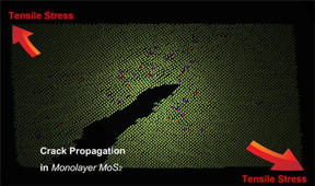 |
| Schematic representation of the crack propagation in 2-D MoS2 at the atomic level. Dislocations shown with red and purple dots are visible at the crack tip zone. Internal tensile stresses are represented by red arrows. CREDIT IBS |
Abstract:
Cracks sank the 'unsinkable' Titanic; decrease the performance of touchscreens and erode teeth. We are familiar with cracks in big or small three-dimensional (3D) objects, but how do thin two-dimensional (2D) materials crack? 2D materials, like molybdenum disulfide (MoS2), have emerged as an important asset for future electronic and photoelectric devices. However, the mechanical properties of 2D materials are expected to differ greatly from 3D materials. Scientists at the Center for Integrated Nanostructure Physics (CINAP), within the Institute for Basic Science (IBS) published, on Nature Communications, the first observation of 2D MoS2 cracking at the atomic level. This study is expected to contribute to the applications of new 2D materials.
Explaining how 2-D materials break at the atomic level
Daejeon, Korea | Posted on January 20th, 2017Obviously when a certain force is applied to a material a crack is created. Less obvious is how to explain and predict the shape and seriousness of a crack from a physics point of view. Scientists want to investigate which fractures are likely to expand and which are not .Materials are divided into ductile and brittle: Ductile materials, like gold, withstand large strains before rupturing; brittle materials, like glass, can absorb relatively little energy before breaking suddenly, without elongation and deformation. At the nano-level atoms move freer in ductile materials than in brittle materials; so in the presence of a pulling force (tensile stress) they can go out of position from the ordered crystal structure, or in technical terms - they dislocate. So far, this explanation (Griffith model) has been applied to cracking phenomena in bulk, but it lacks experimental data at the atomic or nano-scale.
In this study, IBS scientists observed how cracks propagate on 2D MoS2 after a pore was formed either spontaneously or with an electron beam. "The most difficult point {of the experiments} was to use the electron beam to create the pore without generating other defects or breaking the sample," explains Thuc Hue Ly, first author of this study. "So we had to be fast and use a minimum amount of energy."
The atomic observations were done using real-time transmission electron microscopy. Surprisingly, even though MoS2 is a brittle material, the team saw atom dislocations 3-5 nanometers (nm) away from the front line of the crack, or crack tip. This observation cannot be explained with the Griffith model.
In order to create conditions that represent the natural environment, the sample was exposed to ultraviolet (UV) light. This caused the MoS2 to oxidize; atom dislocations occurred more rapidly and the stretched region expanded to 5-10 nm from the crack tip.
"The study shows that cracking in 2D materials is fundamentally different from cracking in 3D ductile and brittle materials. These results cannot be explained with the conventional material failure theory, and we suggest that a new theory is needed," explained Professor LEE Young Hee (CINAP).
####
For more information, please click here
Contacts:
Dahee Carol Kim
Copyright © Institute for Basic Science
If you have a comment, please Contact us.Issuers of news releases, not 7th Wave, Inc. or Nanotechnology Now, are solely responsible for the accuracy of the content.
Bookmark:


| Related Links |
| Related News Press |
News and information
![]() Quantum computer improves AI predictions April 17th, 2026
Quantum computer improves AI predictions April 17th, 2026
![]() Flexible sensor gains sensitivity under pressure April 17th, 2026
Flexible sensor gains sensitivity under pressure April 17th, 2026
![]() A reusable chip for particulate matter sensing April 17th, 2026
A reusable chip for particulate matter sensing April 17th, 2026
![]() Detecting vibrational quantum beating in the predissociation dynamics of SF6 using time-resolved photoelectron spectroscopy April 17th, 2026
Detecting vibrational quantum beating in the predissociation dynamics of SF6 using time-resolved photoelectron spectroscopy April 17th, 2026
2 Dimensional Materials
![]() Flexible sensor gains sensitivity under pressure April 17th, 2026
Flexible sensor gains sensitivity under pressure April 17th, 2026
Possible Futures
![]() A fundamentally new therapeutic approach to cystic fibrosis: Nanobody repairs cellular defect April 17th, 2026
A fundamentally new therapeutic approach to cystic fibrosis: Nanobody repairs cellular defect April 17th, 2026
![]() UC Irvine physicists discover method to reverse �quantum scrambling� : The work addresses the problem of information loss in quantum computing system April 17th, 2026
UC Irvine physicists discover method to reverse �quantum scrambling� : The work addresses the problem of information loss in quantum computing system April 17th, 2026
Chip Technology
![]() A reusable chip for particulate matter sensing April 17th, 2026
A reusable chip for particulate matter sensing April 17th, 2026
![]() Metasurfaces smooth light to boost magnetic sensing precision January 30th, 2026
Metasurfaces smooth light to boost magnetic sensing precision January 30th, 2026
Discoveries
![]() Quantum computer improves AI predictions April 17th, 2026
Quantum computer improves AI predictions April 17th, 2026
![]() Flexible sensor gains sensitivity under pressure April 17th, 2026
Flexible sensor gains sensitivity under pressure April 17th, 2026
![]() A reusable chip for particulate matter sensing April 17th, 2026
A reusable chip for particulate matter sensing April 17th, 2026
![]() Detecting vibrational quantum beating in the predissociation dynamics of SF6 using time-resolved photoelectron spectroscopy April 17th, 2026
Detecting vibrational quantum beating in the predissociation dynamics of SF6 using time-resolved photoelectron spectroscopy April 17th, 2026
Materials/Metamaterials/Magnetoresistance
![]() First real-time observation of two-dimensional melting process: Researchers at Mainz University unveil new insights into magnetic vortex structures August 8th, 2025
First real-time observation of two-dimensional melting process: Researchers at Mainz University unveil new insights into magnetic vortex structures August 8th, 2025
![]() Researchers unveil a groundbreaking clay-based solution to capture carbon dioxide and combat climate change June 6th, 2025
Researchers unveil a groundbreaking clay-based solution to capture carbon dioxide and combat climate change June 6th, 2025
![]() A 1960s idea inspires NBI researchers to study hitherto inaccessible quantum states June 6th, 2025
A 1960s idea inspires NBI researchers to study hitherto inaccessible quantum states June 6th, 2025
![]() Institute for Nanoscience hosts annual proposal planning meeting May 16th, 2025
Institute for Nanoscience hosts annual proposal planning meeting May 16th, 2025
Interviews/Book Reviews/Essays/Reports/Podcasts/Journals/White papers/Posters
![]() A fundamentally new therapeutic approach to cystic fibrosis: Nanobody repairs cellular defect April 17th, 2026
A fundamentally new therapeutic approach to cystic fibrosis: Nanobody repairs cellular defect April 17th, 2026
![]() UC Irvine physicists discover method to reverse �quantum scrambling� : The work addresses the problem of information loss in quantum computing system April 17th, 2026
UC Irvine physicists discover method to reverse �quantum scrambling� : The work addresses the problem of information loss in quantum computing system April 17th, 2026
|
|
||
|
|
||
| The latest news from around the world, FREE | ||
|
|
||
|
|
||
| Premium Products | ||
|
|
||
|
Only the news you want to read!
Learn More |
||
|
|
||
|
Full-service, expert consulting
Learn More |
||
|
|
||