Home > Press > Nanocubes simplify printing and imaging in color and infrared: New technology allows multispectral reactions on a single chip
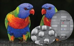 |
| Researchers tested a new technique for printing and imaging in both color and infrared with this image of a parrot. The inlay shows how a simple RGB color scheme was created by building rectangles of varying lengths for each of the colors, as well as individual nanocubes on top of a gold film that create the plasmonic element. CREDIT imageBROKER / Alamy Stock Photo |
Abstract:
Duke University researchers believe they have overcome a longstanding hurdle to producing cheaper, more robust ways to print and image across a range of colors extending into the infrared.
Nanocubes simplify printing and imaging in color and infrared: New technology allows multispectral reactions on a single chip
Durham, NC | Posted on December 15th, 2016As any mantis shrimp will tell you, there are a wide range of "colors" along the electromagnetic spectrum that humans cannot see but which provide a wealth of information. Sensors that extend into the infrared can, for example, identify thousands of plants and minerals, diagnose cancerous melanomas and predict weather patterns, simply by the spectrum of light they reflect.
Current imaging technologies that can detect infrared wavelengths are expensive and bulky, requiring numerous filters or complex assemblies in front of an infrared photodetector. The need for mechanical movement in such devices reduces their expected lifetime and can be a liability in harsh conditions, such as those experienced by satellites.
In a new paper, a team of Duke engineers reveals a manufacturing technique that promises to bring a simplified form of multispectral imaging into daily use. Because the process uses existing materials and fabrication techniques that are inexpensive and easily scalable, it could revolutionize any industry where multispectral imaging or printing is used.
The results appear online December 14 in the journal Advanced Materials.
"It's challenging to create sensors that can detect both the visible spectrum and the infrared," said Maiken Mikkelsen, the Nortel Networks Assistant Professor of Electrical and Computer Engineering and Physics at Duke.
"Traditionally you need different materials that absorb different wavelengths, and that gets very expensive," Mikkelsen said. "But with our technology, the detectors' responses are based on structural properties that we design rather than a material's natural properties. What's really exciting is that we can pair this with a photodetector scheme to combine imaging in both the visible spectrum and the infrared on a single chip."
The new technology relies on plasmonics -- the use of nanoscale physical phenomena to trap certain frequencies of light.
Engineers fashion silver cubes just 100 nanometers wide and place them only a few nanometers above a thin gold foil. When incoming light strikes the surface of a nanocube, it excites the silver's electrons, trapping the light's energy -- but only at a certain frequency.
The size of the silver nanocubes and their distance from the base layer of gold determines that frequency, while controlling the spacing between the nanoparticles allows tuning the strength of the absorption. By precisely tailoring these spacings, researchers can make the system respond to any specific color they want, all the way from visible wavelengths out to the infrared.
The challenge facing the engineers is how to build a useful device that could be scalable and inexpensive enough to use in the real world. For that, Mikkelsen turned to her research team, including graduate student Jon Stewart.
"Similar types of materials have been demonstrated before, but they've all used expensive techniques that have kept the technology from transitioning to the market," said Stewart. "We've come up with a fabrication scheme that is scalable, doesn't need a clean room and avoids using million-dollar machines, all while achieving higher frequency sensitivities. It has allowed us to do things in the field that haven't been done before."
To build a detector, Mikkelsen and Stewart used a process of light etching and adhesives to pattern the nanocubes into pixels containing different sizes of silver nanocubes, and thus each sensitive to a specific wavelength of light. When incoming light strikes the array, each area responds differently depending on the wavelength of light it is sensitive to. By teasing out how each part of the array responds, a computer can reconstruct what color the original light was.
The technique can be used for printing as well, the team showed. Instead of creating pixels with six sections tuned to respond to specific colors, they created pixels with three bars that reflect three colors: blue, green and red. By controlling the relative lengths of each bar, they can dictate what combination of colors the pixel reflects. It's a novel take on the classic RGB scheme first used in photography in 1861.
But unlike most other applications, the plasmonic color scheme promises to never fade over time and can be reliably reproduced with tight accuracy time and again. It also allows its adopters to create color schemes in the infrared.
"Again, the exciting part is being able to print in both visible and infrared on the same substrate," said Mikkelsen. "You could imagine printing an image with a hidden portion in the infrared, or even covering an entire object to tailor its spectral response."
###
This work was supported by the Air Force Office of Scientific Research Young Investigator Research Program (AFOSR, Grant. No. FA9550-15-1-0301).
####
For more information, please click here
Contacts:
Ken Kingery
919-660-8414
Copyright © Duke University
If you have a comment, please Contact us.Issuers of news releases, not 7th Wave, Inc. or Nanotechnology Now, are solely responsible for the accuracy of the content.
Bookmark:


| Related Links |
| Related News Press |
News and information
![]() Quantum computer improves AI predictions April 17th, 2026
Quantum computer improves AI predictions April 17th, 2026
![]() Flexible sensor gains sensitivity under pressure April 17th, 2026
Flexible sensor gains sensitivity under pressure April 17th, 2026
![]() A reusable chip for particulate matter sensing April 17th, 2026
A reusable chip for particulate matter sensing April 17th, 2026
![]() Detecting vibrational quantum beating in the predissociation dynamics of SF6 using time-resolved photoelectron spectroscopy April 17th, 2026
Detecting vibrational quantum beating in the predissociation dynamics of SF6 using time-resolved photoelectron spectroscopy April 17th, 2026
Imaging
![]() Simple algorithm paired with standard imaging tool could predict failure in lithium metal batteries August 8th, 2025
Simple algorithm paired with standard imaging tool could predict failure in lithium metal batteries August 8th, 2025
Govt.-Legislation/Regulation/Funding/Policy
![]() Quantum computer improves AI predictions April 17th, 2026
Quantum computer improves AI predictions April 17th, 2026
![]() Metasurfaces smooth light to boost magnetic sensing precision January 30th, 2026
Metasurfaces smooth light to boost magnetic sensing precision January 30th, 2026
![]() New imaging approach transforms study of bacterial biofilms August 8th, 2025
New imaging approach transforms study of bacterial biofilms August 8th, 2025
Possible Futures
![]() A fundamentally new therapeutic approach to cystic fibrosis: Nanobody repairs cellular defect April 17th, 2026
A fundamentally new therapeutic approach to cystic fibrosis: Nanobody repairs cellular defect April 17th, 2026
![]() UC Irvine physicists discover method to reverse �quantum scrambling� : The work addresses the problem of information loss in quantum computing system April 17th, 2026
UC Irvine physicists discover method to reverse �quantum scrambling� : The work addresses the problem of information loss in quantum computing system April 17th, 2026
Discoveries
![]() Quantum computer improves AI predictions April 17th, 2026
Quantum computer improves AI predictions April 17th, 2026
![]() Flexible sensor gains sensitivity under pressure April 17th, 2026
Flexible sensor gains sensitivity under pressure April 17th, 2026
![]() A reusable chip for particulate matter sensing April 17th, 2026
A reusable chip for particulate matter sensing April 17th, 2026
![]() Detecting vibrational quantum beating in the predissociation dynamics of SF6 using time-resolved photoelectron spectroscopy April 17th, 2026
Detecting vibrational quantum beating in the predissociation dynamics of SF6 using time-resolved photoelectron spectroscopy April 17th, 2026
Announcements
![]() A fundamentally new therapeutic approach to cystic fibrosis: Nanobody repairs cellular defect April 17th, 2026
A fundamentally new therapeutic approach to cystic fibrosis: Nanobody repairs cellular defect April 17th, 2026
![]() UC Irvine physicists discover method to reverse �quantum scrambling� : The work addresses the problem of information loss in quantum computing system April 17th, 2026
UC Irvine physicists discover method to reverse �quantum scrambling� : The work addresses the problem of information loss in quantum computing system April 17th, 2026
Interviews/Book Reviews/Essays/Reports/Podcasts/Journals/White papers/Posters
![]() A fundamentally new therapeutic approach to cystic fibrosis: Nanobody repairs cellular defect April 17th, 2026
A fundamentally new therapeutic approach to cystic fibrosis: Nanobody repairs cellular defect April 17th, 2026
![]() UC Irvine physicists discover method to reverse �quantum scrambling� : The work addresses the problem of information loss in quantum computing system April 17th, 2026
UC Irvine physicists discover method to reverse �quantum scrambling� : The work addresses the problem of information loss in quantum computing system April 17th, 2026
Military
![]() Quantum engineers �squeeze� laser frequency combs to make more sensitive gas sensors January 17th, 2025
Quantum engineers �squeeze� laser frequency combs to make more sensitive gas sensors January 17th, 2025
![]() Chainmail-like material could be the future of armor: First 2D mechanically interlocked polymer exhibits exceptional flexibility and strength January 17th, 2025
Chainmail-like material could be the future of armor: First 2D mechanically interlocked polymer exhibits exceptional flexibility and strength January 17th, 2025
![]() Single atoms show their true color July 5th, 2024
Single atoms show their true color July 5th, 2024
![]() NRL charters Navy�s quantum inertial navigation path to reduce drift April 5th, 2024
NRL charters Navy�s quantum inertial navigation path to reduce drift April 5th, 2024
Printing/Lithography/Inkjet/Inks/Bio-printing/Dyes
![]() Presenting: Ultrasound-based printing of 3D materials�potentially inside the body December 8th, 2023
Presenting: Ultrasound-based printing of 3D materials�potentially inside the body December 8th, 2023
![]() Simple ballpoint pen can write custom LEDs August 11th, 2023
Simple ballpoint pen can write custom LEDs August 11th, 2023
![]() Disposable electronics on a simple sheet of paper October 7th, 2022
Disposable electronics on a simple sheet of paper October 7th, 2022
|
|
||
|
|
||
| The latest news from around the world, FREE | ||
|
|
||
|
|
||
| Premium Products | ||
|
|
||
|
Only the news you want to read!
Learn More |
||
|
|
||
|
Full-service, expert consulting
Learn More |
||
|
|
||