Home > Press > New optofluidic platform features tunable optics and novel 'lightvalves': UC Santa Cruz engineers use flexible silicone material to build an integrated optofluidic platform for biological sample processing and optical analysis
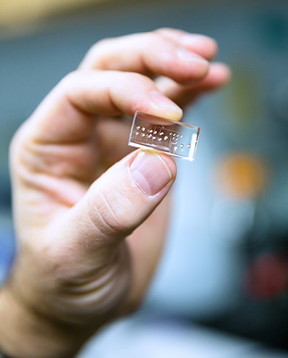 |
| A new optofluidic platform for biological sample processing and optical analysis is made of polydimethylsiloxane (PDMS) and features tunable optics and novel 'lightvalves.' Photo by C. Lagattuta |
Abstract:
For well over a decade, electrical engineer Holger Schmidt has been developing devices for optical analysis of samples on integrated chip-based platforms, with applications in areas such as biological sensors, virus detection, and chemical analysis. The latest device from his lab is based on novel technology that combines high-performance microfluidics for sample processing with dynamic optical tuning and switching, all on a low-cost "chip" made of a flexible silicone material.
New optofluidic platform features tunable optics and novel 'lightvalves': UC Santa Cruz engineers use flexible silicone material to build an integrated optofluidic platform for biological sample processing and optical analysis
Santa Cruz, CA | Posted on September 15th, 2016In previous devices from Schmidt's lab, optical functions were built into silicon chips using the same fabrication technology used to make computer chips. The new device is made entirely of polydimethylsiloxane (PDMS), a soft, flexible material used in microfluidics as well as in products such as contact lenses and medical devices.
"We can use this fabrication method now to build an all-in-one device that allows us to do biological sample processing and optical detection on one chip," said Schmidt, the Kapany Professor of Optoelectronics and director of the W. M. Keck Center for Nanoscale Optofluidics at UC Santa Cruz.
The flexibility of PDMS allows for novel ways of controlling both light and fluids on the chip. Using multilayer soft lithography techniques, senior graduate student Joshua Parks built chips containing both solid-core and hollow-core waveguides for guiding light signals, as well as fluidic microvalves to control the movement of liquid samples. Schmidt and Parks also developed a special microvalve that functions as a "lightvalve," controlling the flow of both light and fluids.
"That opens up a whole new set of functions that we couldn't do on a silicon chip," Schmidt said. "The lightvalve is the most exciting element. In additional to a simple on-off switch, we built a moveable optical trap for analysis of biological particles such as viruses or bacteria."
In a previous study, Schmidt, Parks, and colleagues at BYU and UC Berkeley demonstrated a hybrid device in which a PDMS microfluidic chip for sample preparation was integrated with a silicon-based optofluidic chip for optical detection of viral pathogens. The new device combines both functions on the same chip. In addition, Schmidt said, the materials are relatively inexpensive, allowing rapid prototyping of devices.
"We can do the full chain of fabrication here in our lab, and we can make new devices very quickly," he said.
Schmidt said the potential applications for this technology include a wide range of biological sensors and analytical devices. For viral diagnostic assays, for example, fluorescently labeled antibodies can be used to tag specific viral strains for optical detection. In a recent paper, Schmidt and colleagues demonstrated detection and identification of different flu strains using fluorescence detection in a multi-mode interference (MMI) waveguide. With the new device, they showed that they can actively tune an MMI waveguide on the chip.
The dynamic tuning of the optofluidic device is achieved by applying pressure to the optofluidic channel, changing its dimensions and thereby altering its photonic properties. "We can actually tune the spot pattern made in the channel by the interference waveguide, which we couldn't do with the silicon chip," Schmidt said.
This work was supported by grants from the National Science Foundation and National Institutes of Health.
####
For more information, please click here
Contacts:
Tim Stephens
(831) 459-4352
Holger Schmidt
831) 459-1482
Copyright © UC Santa Cruz
If you have a comment, please Contact us.Issuers of news releases, not 7th Wave, Inc. or Nanotechnology Now, are solely responsible for the accuracy of the content.
Bookmark:


| Related Links |
| Related News Press |
News and information
![]() Quantum computer improves AI predictions April 17th, 2026
Quantum computer improves AI predictions April 17th, 2026
![]() Flexible sensor gains sensitivity under pressure April 17th, 2026
Flexible sensor gains sensitivity under pressure April 17th, 2026
![]() A reusable chip for particulate matter sensing April 17th, 2026
A reusable chip for particulate matter sensing April 17th, 2026
![]() Detecting vibrational quantum beating in the predissociation dynamics of SF6 using time-resolved photoelectron spectroscopy April 17th, 2026
Detecting vibrational quantum beating in the predissociation dynamics of SF6 using time-resolved photoelectron spectroscopy April 17th, 2026
Govt.-Legislation/Regulation/Funding/Policy
![]() Quantum computer improves AI predictions April 17th, 2026
Quantum computer improves AI predictions April 17th, 2026
![]() Metasurfaces smooth light to boost magnetic sensing precision January 30th, 2026
Metasurfaces smooth light to boost magnetic sensing precision January 30th, 2026
![]() New imaging approach transforms study of bacterial biofilms August 8th, 2025
New imaging approach transforms study of bacterial biofilms August 8th, 2025
Possible Futures
![]() A fundamentally new therapeutic approach to cystic fibrosis: Nanobody repairs cellular defect April 17th, 2026
A fundamentally new therapeutic approach to cystic fibrosis: Nanobody repairs cellular defect April 17th, 2026
![]() UC Irvine physicists discover method to reverse �quantum scrambling� : The work addresses the problem of information loss in quantum computing system April 17th, 2026
UC Irvine physicists discover method to reverse �quantum scrambling� : The work addresses the problem of information loss in quantum computing system April 17th, 2026
Optical computing/Photonic computing
![]() ICFO researchers overcome long-standing bottleneck in single photon detection with twisted 2D materials August 8th, 2025
ICFO researchers overcome long-standing bottleneck in single photon detection with twisted 2D materials August 8th, 2025
![]() Programmable electron-induced color router array May 14th, 2025
Programmable electron-induced color router array May 14th, 2025
Discoveries
![]() Quantum computer improves AI predictions April 17th, 2026
Quantum computer improves AI predictions April 17th, 2026
![]() Flexible sensor gains sensitivity under pressure April 17th, 2026
Flexible sensor gains sensitivity under pressure April 17th, 2026
![]() A reusable chip for particulate matter sensing April 17th, 2026
A reusable chip for particulate matter sensing April 17th, 2026
![]() Detecting vibrational quantum beating in the predissociation dynamics of SF6 using time-resolved photoelectron spectroscopy April 17th, 2026
Detecting vibrational quantum beating in the predissociation dynamics of SF6 using time-resolved photoelectron spectroscopy April 17th, 2026
Announcements
![]() A fundamentally new therapeutic approach to cystic fibrosis: Nanobody repairs cellular defect April 17th, 2026
A fundamentally new therapeutic approach to cystic fibrosis: Nanobody repairs cellular defect April 17th, 2026
![]() UC Irvine physicists discover method to reverse �quantum scrambling� : The work addresses the problem of information loss in quantum computing system April 17th, 2026
UC Irvine physicists discover method to reverse �quantum scrambling� : The work addresses the problem of information loss in quantum computing system April 17th, 2026
Interviews/Book Reviews/Essays/Reports/Podcasts/Journals/White papers/Posters
![]() A fundamentally new therapeutic approach to cystic fibrosis: Nanobody repairs cellular defect April 17th, 2026
A fundamentally new therapeutic approach to cystic fibrosis: Nanobody repairs cellular defect April 17th, 2026
![]() UC Irvine physicists discover method to reverse �quantum scrambling� : The work addresses the problem of information loss in quantum computing system April 17th, 2026
UC Irvine physicists discover method to reverse �quantum scrambling� : The work addresses the problem of information loss in quantum computing system April 17th, 2026
Photonics/Optics/Lasers
![]() Metasurfaces smooth light to boost magnetic sensing precision January 30th, 2026
Metasurfaces smooth light to boost magnetic sensing precision January 30th, 2026
![]() From sensors to smart systems: the rise of AI-driven photonic noses January 30th, 2026
From sensors to smart systems: the rise of AI-driven photonic noses January 30th, 2026
|
|
||
|
|
||
| The latest news from around the world, FREE | ||
|
|
||
|
|
||
| Premium Products | ||
|
|
||
|
Only the news you want to read!
Learn More |
||
|
|
||
|
Full-service, expert consulting
Learn More |
||
|
|
||