Home > Press > NREL theory establishes a path to high-performance 2-D semiconductor devices
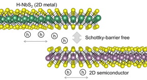 |
| Using 2D metal as contact for 2D semiconductor allows Schottky barrier to be tuned, due to the weak Fermi level pinning at the junction caused by the suppression of metal-induced gap states. Schematic illustrates that 2D H-NbS2 can form a Schottky-barrier-free contact with 2D semiconductor for hole transport. Credit: National Renewable Energy Laboratory |
Abstract:
Researchers at the Energy Department's National Renewable Energy Laboratory (NREL) have uncovered a way to overcome a principal obstacle in using two-dimensional (2D) semiconductors in electronic and optoelectronic devices.
NREL theory establishes a path to high-performance 2-D semiconductor devices
Golden, CO | Posted on April 27th, 20162D semiconductors such as molybdenum disulfide are only a few layers thick and are considered promising candidates for next-generation devices. Scientists first must overcome limitations imposed by a large and tunable Schottky barrier between the semiconductor and a metal contact. The barrier, at the metal/semiconductor junction, creates an obstacle for the flow of electrons or holes through the semiconductor.
The NREL team discovered that the height of the Schottky barrier can be adjusted-or even made to vanish-by using certain 2D metals as electrodes. Such adjustments are not possible with conventional three-dimensional metals because of a strong Fermi level pinning (FLP) effect occurring at the junction of metal and semiconductor, due to electronic states in the semiconductor band gap that are induced by the metal. Increasing the flow of electrons or holes through a semiconductor reduces power losses and improves the device performance.
The NREL theorists considered a family of 2D metals that could bind with the 2D semiconductors through van der Waals interaction. Because this interaction is relatively weak, the metal-induced gap states are suppressed and the FLP effect is negligible. This means that the Schottky barrier becomes highly tunable. By selecting an appropriate 2D metal/2D semiconductor pair, one can reduce the barrier to almost zero (such as H-NbS2/WSe2 for hole conduction).
They noted that using a 2D metal as an electrode would also prove useful for integrating into transparent and flexible electronics because the 2D metal is also transparent and flexible. They also noted that the junction of 2D metal and 2D semiconductor is atomically flat and can have fewer defects, which would reduce carrier scattering and recombination.
The work by Yuanyue Liu, Paul Stradins, and Su-Huai Wei, "Van der Waals metal-semiconductor junction: weak Fermi level pinning enables effective tuning of Schottky barrier," appears in the new issue of Science Advances.
The trio of researchers predicts that hexagonal phase of niobium disulfide (NbS2) is the most promising for hole injection into a 2D semiconductor, and heavily nitrogen-doped graphene can enable efficient electron injection.
###
This research was funded by the Department of Energy's Office of Energy Efficiency and Renewable Energy. The work used computational resources at NREL and the National Energy Research Scientific Computing Center.
####
About National Renewable Energy Laboratory
NREL is the U.S. Department of Energy's primary national laboratory for renewable energy and energy efficiency research and development. NREL is operated for the Energy Department by The Alliance for Sustainable Energy, LLC.
For more information, please click here
Contacts:
David Glickson
303-275-4097
Copyright © National Renewable Energy Laboratory
If you have a comment, please Contact us.Issuers of news releases, not 7th Wave, Inc. or Nanotechnology Now, are solely responsible for the accuracy of the content.
Bookmark:


| Related Links |
| Related News Press |
News and information
![]() Quantum computer improves AI predictions April 17th, 2026
Quantum computer improves AI predictions April 17th, 2026
![]() Flexible sensor gains sensitivity under pressure April 17th, 2026
Flexible sensor gains sensitivity under pressure April 17th, 2026
![]() A reusable chip for particulate matter sensing April 17th, 2026
A reusable chip for particulate matter sensing April 17th, 2026
![]() Detecting vibrational quantum beating in the predissociation dynamics of SF6 using time-resolved photoelectron spectroscopy April 17th, 2026
Detecting vibrational quantum beating in the predissociation dynamics of SF6 using time-resolved photoelectron spectroscopy April 17th, 2026
2 Dimensional Materials
![]() Flexible sensor gains sensitivity under pressure April 17th, 2026
Flexible sensor gains sensitivity under pressure April 17th, 2026
![]() ICFO researchers overcome long-standing bottleneck in single photon detection with twisted 2D materials August 8th, 2025
ICFO researchers overcome long-standing bottleneck in single photon detection with twisted 2D materials August 8th, 2025
![]() First real-time observation of two-dimensional melting process: Researchers at Mainz University unveil new insights into magnetic vortex structures August 8th, 2025
First real-time observation of two-dimensional melting process: Researchers at Mainz University unveil new insights into magnetic vortex structures August 8th, 2025
![]() Lab to industry: InSe wafer-scale breakthrough for future electronics August 8th, 2025
Lab to industry: InSe wafer-scale breakthrough for future electronics August 8th, 2025
Laboratories
![]() Researchers develop molecular qubits that communicate at telecom frequencies October 3rd, 2025
Researchers develop molecular qubits that communicate at telecom frequencies October 3rd, 2025
Hardware
![]() The present and future of computing get a boost from new research July 21st, 2023
The present and future of computing get a boost from new research July 21st, 2023
![]() A Carbon Nanotube Microprocessor Mature Enough to Say Hello: Three new breakthroughs make commercial nanotube processors possible March 2nd, 2020
A Carbon Nanotube Microprocessor Mature Enough to Say Hello: Three new breakthroughs make commercial nanotube processors possible March 2nd, 2020
![]() Powering the future: Smallest all-digital circuit opens doors to 5 nm next-gen semiconductor February 11th, 2020
Powering the future: Smallest all-digital circuit opens doors to 5 nm next-gen semiconductor February 11th, 2020
Govt.-Legislation/Regulation/Funding/Policy
![]() Quantum computer improves AI predictions April 17th, 2026
Quantum computer improves AI predictions April 17th, 2026
![]() Metasurfaces smooth light to boost magnetic sensing precision January 30th, 2026
Metasurfaces smooth light to boost magnetic sensing precision January 30th, 2026
![]() New imaging approach transforms study of bacterial biofilms August 8th, 2025
New imaging approach transforms study of bacterial biofilms August 8th, 2025
Possible Futures
![]() A fundamentally new therapeutic approach to cystic fibrosis: Nanobody repairs cellular defect April 17th, 2026
A fundamentally new therapeutic approach to cystic fibrosis: Nanobody repairs cellular defect April 17th, 2026
![]() UC Irvine physicists discover method to reverse �quantum scrambling� : The work addresses the problem of information loss in quantum computing system April 17th, 2026
UC Irvine physicists discover method to reverse �quantum scrambling� : The work addresses the problem of information loss in quantum computing system April 17th, 2026
Chip Technology
![]() A reusable chip for particulate matter sensing April 17th, 2026
A reusable chip for particulate matter sensing April 17th, 2026
![]() Metasurfaces smooth light to boost magnetic sensing precision January 30th, 2026
Metasurfaces smooth light to boost magnetic sensing precision January 30th, 2026
Optical computing/Photonic computing
![]() ICFO researchers overcome long-standing bottleneck in single photon detection with twisted 2D materials August 8th, 2025
ICFO researchers overcome long-standing bottleneck in single photon detection with twisted 2D materials August 8th, 2025
![]() Programmable electron-induced color router array May 14th, 2025
Programmable electron-induced color router array May 14th, 2025
Discoveries
![]() Quantum computer improves AI predictions April 17th, 2026
Quantum computer improves AI predictions April 17th, 2026
![]() Flexible sensor gains sensitivity under pressure April 17th, 2026
Flexible sensor gains sensitivity under pressure April 17th, 2026
![]() A reusable chip for particulate matter sensing April 17th, 2026
A reusable chip for particulate matter sensing April 17th, 2026
![]() Detecting vibrational quantum beating in the predissociation dynamics of SF6 using time-resolved photoelectron spectroscopy April 17th, 2026
Detecting vibrational quantum beating in the predissociation dynamics of SF6 using time-resolved photoelectron spectroscopy April 17th, 2026
Announcements
![]() A fundamentally new therapeutic approach to cystic fibrosis: Nanobody repairs cellular defect April 17th, 2026
A fundamentally new therapeutic approach to cystic fibrosis: Nanobody repairs cellular defect April 17th, 2026
![]() UC Irvine physicists discover method to reverse �quantum scrambling� : The work addresses the problem of information loss in quantum computing system April 17th, 2026
UC Irvine physicists discover method to reverse �quantum scrambling� : The work addresses the problem of information loss in quantum computing system April 17th, 2026
Interviews/Book Reviews/Essays/Reports/Podcasts/Journals/White papers/Posters
![]() A fundamentally new therapeutic approach to cystic fibrosis: Nanobody repairs cellular defect April 17th, 2026
A fundamentally new therapeutic approach to cystic fibrosis: Nanobody repairs cellular defect April 17th, 2026
![]() UC Irvine physicists discover method to reverse �quantum scrambling� : The work addresses the problem of information loss in quantum computing system April 17th, 2026
UC Irvine physicists discover method to reverse �quantum scrambling� : The work addresses the problem of information loss in quantum computing system April 17th, 2026
Photonics/Optics/Lasers
![]() Metasurfaces smooth light to boost magnetic sensing precision January 30th, 2026
Metasurfaces smooth light to boost magnetic sensing precision January 30th, 2026
![]() From sensors to smart systems: the rise of AI-driven photonic noses January 30th, 2026
From sensors to smart systems: the rise of AI-driven photonic noses January 30th, 2026
|
|
||
|
|
||
| The latest news from around the world, FREE | ||
|
|
||
|
|
||
| Premium Products | ||
|
|
||
|
Only the news you want to read!
Learn More |
||
|
|
||
|
Full-service, expert consulting
Learn More |
||
|
|
||