Home > Press > Controlling integrated optical circuits using patterns of light
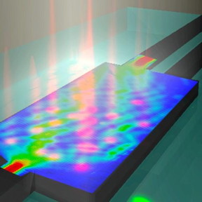 |
| The image shows an artistic rendering of a silicon-on-insulator 1x2 multimode interference splitter with a projected pattern of perturbations induced by femtosecond laser. The perturbation pattern achieves routing of light to a single output port with 97 percent efficiency. CREDIT: University of Southampton |
Abstract:
Researchers from the University of Southampton (UK), and the Institut d'Optique in Bordeaux (France) have devised a new approach for controlling light in a silicon chip by bringing the concept of spatial light modulation to integrated optics.
Controlling integrated optical circuits using patterns of light
Southampton, UK | Posted on April 19th, 2016Silicon photonics are forming the backbone of next-generation on-chip technologies and optical telecommunication, which are aimed at a wide range of emerging applications including optical interconnects, microwave photonic circuits, and integrated optical sensors.
Photonic chip functionality is usually hard-wired by design, however reconfigurable optical elements would allow light to be routed flexibly, opening up new applications in programmable photonic circuits.
Traditional spatial light modulators are based on liquid crystals or micromirrors and provide many independently controllable pixels. This technology has revolutionised optics in recent years, with many applications in imaging and holography, adaptive optics and wavefront shaping of light through opaque media.
In their new work, presented in the April issue of the journal Optica, the team makes use of multimode interference (MMI) devices, which form a versatile class of integrated optical elements routinely used for splitting and recombining different signals on a chip. The geometry of the MMI predefines its characteristics at the fabrication stage.
The team shows that the intricate interplay between many modes travelling through the MMI can be dynamically controlled. A pattern of local perturbations, induced by femtosecond laser, acts in concert to effectively shape the transmitted light. Related to wavefront shaping in free-space optics, this allows to freely route light in a static silicon element, thus transforming the device into a much needed building block for field-programmable photonics.
Lead author Roman Bruck, a postdoctoral researcher at the University of Southampton, says: "We have demonstrated a very general approach to beam shaping on a chip that provides a wide range of useful functionalities to integrated circuits. The integrated spatial light modulator turns conventional silicon photonics components into versatile reconfigurable elements."
Practical applications of this technology will include all-optical reconfigurable routers, ultrafast optical modulators and switches for optical networks and microwave photonic circuits as well as wafer-scale optical testing of photonic chips. More work is needed to develop these ideas into practical applications.
Principal investigator Professor Otto Muskens, from Physics and Astronomy at the University of Southampton, says: "There are many new directions to explore, from gaining a deeper understanding to application of the new concepts into real-world devices. This is a potentially disruptive new approach toward field-programmable chips which can enhance and complement existing strategies, or even partially replace current technology."
####
For more information, please click here
Contacts:
Glenn Harris
44-023-805-93212
Copyright © University of Southampton
If you have a comment, please Contact us.Issuers of news releases, not 7th Wave, Inc. or Nanotechnology Now, are solely responsible for the accuracy of the content.
Bookmark:


| Related Links |
| Related News Press |
News and information
![]() Quantum computer improves AI predictions April 17th, 2026
Quantum computer improves AI predictions April 17th, 2026
![]() Flexible sensor gains sensitivity under pressure April 17th, 2026
Flexible sensor gains sensitivity under pressure April 17th, 2026
![]() A reusable chip for particulate matter sensing April 17th, 2026
A reusable chip for particulate matter sensing April 17th, 2026
![]() Detecting vibrational quantum beating in the predissociation dynamics of SF6 using time-resolved photoelectron spectroscopy April 17th, 2026
Detecting vibrational quantum beating in the predissociation dynamics of SF6 using time-resolved photoelectron spectroscopy April 17th, 2026
Possible Futures
![]() A fundamentally new therapeutic approach to cystic fibrosis: Nanobody repairs cellular defect April 17th, 2026
A fundamentally new therapeutic approach to cystic fibrosis: Nanobody repairs cellular defect April 17th, 2026
![]() UC Irvine physicists discover method to reverse �quantum scrambling� : The work addresses the problem of information loss in quantum computing system April 17th, 2026
UC Irvine physicists discover method to reverse �quantum scrambling� : The work addresses the problem of information loss in quantum computing system April 17th, 2026
Chip Technology
![]() A reusable chip for particulate matter sensing April 17th, 2026
A reusable chip for particulate matter sensing April 17th, 2026
![]() Metasurfaces smooth light to boost magnetic sensing precision January 30th, 2026
Metasurfaces smooth light to boost magnetic sensing precision January 30th, 2026
Optical computing/Photonic computing
![]() ICFO researchers overcome long-standing bottleneck in single photon detection with twisted 2D materials August 8th, 2025
ICFO researchers overcome long-standing bottleneck in single photon detection with twisted 2D materials August 8th, 2025
![]() Programmable electron-induced color router array May 14th, 2025
Programmable electron-induced color router array May 14th, 2025
Discoveries
![]() Quantum computer improves AI predictions April 17th, 2026
Quantum computer improves AI predictions April 17th, 2026
![]() Flexible sensor gains sensitivity under pressure April 17th, 2026
Flexible sensor gains sensitivity under pressure April 17th, 2026
![]() A reusable chip for particulate matter sensing April 17th, 2026
A reusable chip for particulate matter sensing April 17th, 2026
![]() Detecting vibrational quantum beating in the predissociation dynamics of SF6 using time-resolved photoelectron spectroscopy April 17th, 2026
Detecting vibrational quantum beating in the predissociation dynamics of SF6 using time-resolved photoelectron spectroscopy April 17th, 2026
Announcements
![]() A fundamentally new therapeutic approach to cystic fibrosis: Nanobody repairs cellular defect April 17th, 2026
A fundamentally new therapeutic approach to cystic fibrosis: Nanobody repairs cellular defect April 17th, 2026
![]() UC Irvine physicists discover method to reverse �quantum scrambling� : The work addresses the problem of information loss in quantum computing system April 17th, 2026
UC Irvine physicists discover method to reverse �quantum scrambling� : The work addresses the problem of information loss in quantum computing system April 17th, 2026
Interviews/Book Reviews/Essays/Reports/Podcasts/Journals/White papers/Posters
![]() A fundamentally new therapeutic approach to cystic fibrosis: Nanobody repairs cellular defect April 17th, 2026
A fundamentally new therapeutic approach to cystic fibrosis: Nanobody repairs cellular defect April 17th, 2026
![]() UC Irvine physicists discover method to reverse �quantum scrambling� : The work addresses the problem of information loss in quantum computing system April 17th, 2026
UC Irvine physicists discover method to reverse �quantum scrambling� : The work addresses the problem of information loss in quantum computing system April 17th, 2026
Photonics/Optics/Lasers
![]() Metasurfaces smooth light to boost magnetic sensing precision January 30th, 2026
Metasurfaces smooth light to boost magnetic sensing precision January 30th, 2026
![]() From sensors to smart systems: the rise of AI-driven photonic noses January 30th, 2026
From sensors to smart systems: the rise of AI-driven photonic noses January 30th, 2026
Research partnerships
![]() Lab to industry: InSe wafer-scale breakthrough for future electronics August 8th, 2025
Lab to industry: InSe wafer-scale breakthrough for future electronics August 8th, 2025
![]() HKU physicists uncover hidden order in the quantum world through deconfined quantum critical points April 25th, 2025
HKU physicists uncover hidden order in the quantum world through deconfined quantum critical points April 25th, 2025
|
|
||
|
|
||
| The latest news from around the world, FREE | ||
|
|
||
|
|
||
| Premium Products | ||
|
|
||
|
Only the news you want to read!
Learn More |
||
|
|
||
|
Full-service, expert consulting
Learn More |
||
|
|
||