Home > Press > 'Odd couple' monolayer semiconductors align to advance optoelectronics
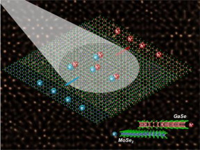 |
| Light drives the migration of charge carriers (electrons and holes) at the juncture between semiconductors with mismatched crystal lattices. These heterostructures hold promise for advancing optoelectronics and exploring new physics. The schematic's background is a scanning transmission electron microscope image showing the bilayer in atomic-scale resolution. CREDIT: Oak Ridge National Laboratory, US Dept. of Energy. Image by Xufan Li and Chris Rouleau |
Abstract:
Epitaxy, or growing crystalline film layers that are templated by a crystalline substrate, is a mainstay of manufacturing transistors and semiconductors. If the material in one deposited layer is the same as the material in the next layer, it can be energetically favorable for strong bonds to form between the highly ordered, perfectly matched layers. In contrast, trying to layer dissimilar materials is a great challenge if the crystal lattices don't match up easily. Then, weak van der Waals forces create attraction but don't form strong bonds between unlike layers.
'Odd couple' monolayer semiconductors align to advance optoelectronics
Oak Ridge, TN | Posted on April 18th, 2016In a study led by the Department of Energy's Oak Ridge National Laboratory, scientists synthesized a stack of atomically thin monolayers of two lattice-mismatched semiconductors. One, gallium selenide, is a "p-type" semiconductor, rich in charge carriers called "holes." The other, molybdenum diselenide, is an "n-type" semiconductor, rich in electron charge carriers. Where the two semiconductor layers met, they formed an atomically sharp heterostructure called a p-n junction, which generated a photovoltaic response by separating electron-hole pairs that were generated by light. The achievement of creating this atomically thin solar cell, published in Science Advances, shows the promise of synthesizing mismatched layers to enable new families of functional two-dimensional (2D) materials.
The idea of stacking different materials on top of each other isn't new by itself. In fact, it is the basis for most electronic devices in use today. But such stacking usually only works when the individual materials have crystal lattices that are very similar, i.e., they have a good "lattice match." This is where this research breaks new ground by growing high-quality layers of very different 2D materials, broadening the number of materials that can be combined and thus creating a wider range of potential atomically thin electronic devices.
"Because the two layers had such a large lattice mismatch between them, it's very unexpected that they would grow on each other in an orderly way," said ORNL's Xufan Li, lead author of the study. "But it worked."
The group was the first to show that monolayers of two different types of metal chalcogenides--binary compounds of sulfur, selenium or tellurium with a more electropositive element or radical--having such different lattice constants can be grown together to form a perfectly aligned stacking bilayer. "It's a new, potential building block for energy-efficient optoelectronics," Li said.
Upon characterizing their new bilayer building block, the researchers found that the two mismatched layers had self-assembled into a repeating long-range atomic order that could be directly visualized by the Moir� patterns they showed in the electron microscope. "We were surprised that these patterns aligned perfectly," Li said.
Researchers in ORNL's Functional Hybrid Nanomaterials group, led by David Geohegan, conducted the study with partners at Vanderbilt University, the University of Utah and Beijing Computational Science Research Center.
"These new 2D mismatched layered heterostructures open the door to novel building blocks for optoelectronic applications," said senior author Kai Xiao of ORNL. "They can allow us to study new physics properties which cannot be discovered with other 2D heterostructures with matched lattices. They offer potential for a wide range of physical phenomena ranging from interfacial magnetism, superconductivity and Hofstadter's butterfly effect."
Li first grew a monolayer of molybdenum diselenide, and then grew a layer of gallium selenide on top. This technique, called "van der Waals epitaxy," is named for the weak attractive forces that hold dissimilar layers together. "With van der Waals epitaxy, despite big lattice mismatches, you can still grow another layer on the first," Li said. Using scanning transmission electron microscopy, the team characterized the atomic structure of the materials and revealed the formation of Moir� patterns.
The scientists plan to conduct future studies to explore how the material aligns during the growth process and how material composition influences properties beyond the photovoltaic response. The research advances efforts to incorporate 2D materials into devices.
For many years, layering different compounds with similar lattice cell sizes has been widely studied. Different elements have been incorporated into the compounds to produce a wide range of physical properties related to superconductivity, magnetism and thermoelectrics. But layering 2D compounds having dissimilar lattice cell sizes is virtually unexplored territory.
"We've opened the door to exploring all types of mismatched heterostructures," Li said.
The title of the paper is "Two-dimensional GaSe/MoSe2 misfit bilayer heterojunctions by van der Waals epitaxy."
###
Research, including materials synthesis, was supported by the DOE Office of Science. Materials characterization was conducted in part at the Center for Nanophase Materials Sciences, a DOE Office of Science User Facility at ORNL. ORNL Laboratory Directed Research and Development funds supported some of the device measurements in the study.
####
About Oak Ridge National Laboratory
UT-Battelle manages ORNL for DOE's Office of Science. The single largest supporter of basic research in the physical sciences in the United States, the Office of Science is working to address some of the most pressing challenges of our time.
For more information, please click here
Contacts:
Dawn Levy
865-576-6448
Copyright © Oak Ridge National Laboratory
If you have a comment, please Contact us.Issuers of news releases, not 7th Wave, Inc. or Nanotechnology Now, are solely responsible for the accuracy of the content.
Bookmark:


| Related Links |
| Related News Press |
News and information
![]() Quantum computer improves AI predictions April 17th, 2026
Quantum computer improves AI predictions April 17th, 2026
![]() Flexible sensor gains sensitivity under pressure April 17th, 2026
Flexible sensor gains sensitivity under pressure April 17th, 2026
![]() A reusable chip for particulate matter sensing April 17th, 2026
A reusable chip for particulate matter sensing April 17th, 2026
![]() Detecting vibrational quantum beating in the predissociation dynamics of SF6 using time-resolved photoelectron spectroscopy April 17th, 2026
Detecting vibrational quantum beating in the predissociation dynamics of SF6 using time-resolved photoelectron spectroscopy April 17th, 2026
2 Dimensional Materials
![]() Flexible sensor gains sensitivity under pressure April 17th, 2026
Flexible sensor gains sensitivity under pressure April 17th, 2026
![]() MXene nanomaterials enter a new dimension Multilayer nanomaterial: MXene flakes created at Drexel University show new promise as 1D scrolls January 30th, 2026
MXene nanomaterials enter a new dimension Multilayer nanomaterial: MXene flakes created at Drexel University show new promise as 1D scrolls January 30th, 2026
![]() ICFO researchers overcome long-standing bottleneck in single photon detection with twisted 2D materials August 8th, 2025
ICFO researchers overcome long-standing bottleneck in single photon detection with twisted 2D materials August 8th, 2025
Imaging
![]() Simple algorithm paired with standard imaging tool could predict failure in lithium metal batteries August 8th, 2025
Simple algorithm paired with standard imaging tool could predict failure in lithium metal batteries August 8th, 2025
![]() First real-time observation of two-dimensional melting process: Researchers at Mainz University unveil new insights into magnetic vortex structures August 8th, 2025
First real-time observation of two-dimensional melting process: Researchers at Mainz University unveil new insights into magnetic vortex structures August 8th, 2025
Thin films
![]() Tiny nanosheets, big leap: A new sensor detects ethanol at ultra-low levels January 30th, 2026
Tiny nanosheets, big leap: A new sensor detects ethanol at ultra-low levels January 30th, 2026
Laboratories
![]() Researchers develop molecular qubits that communicate at telecom frequencies October 3rd, 2025
Researchers develop molecular qubits that communicate at telecom frequencies October 3rd, 2025
Govt.-Legislation/Regulation/Funding/Policy
![]() Quantum computer improves AI predictions April 17th, 2026
Quantum computer improves AI predictions April 17th, 2026
![]() Metasurfaces smooth light to boost magnetic sensing precision January 30th, 2026
Metasurfaces smooth light to boost magnetic sensing precision January 30th, 2026
![]() New imaging approach transforms study of bacterial biofilms August 8th, 2025
New imaging approach transforms study of bacterial biofilms August 8th, 2025
Possible Futures
![]() A fundamentally new therapeutic approach to cystic fibrosis: Nanobody repairs cellular defect April 17th, 2026
A fundamentally new therapeutic approach to cystic fibrosis: Nanobody repairs cellular defect April 17th, 2026
![]() UC Irvine physicists discover method to reverse �quantum scrambling� : The work addresses the problem of information loss in quantum computing system April 17th, 2026
UC Irvine physicists discover method to reverse �quantum scrambling� : The work addresses the problem of information loss in quantum computing system April 17th, 2026
Chip Technology
![]() A reusable chip for particulate matter sensing April 17th, 2026
A reusable chip for particulate matter sensing April 17th, 2026
![]() Metasurfaces smooth light to boost magnetic sensing precision January 30th, 2026
Metasurfaces smooth light to boost magnetic sensing precision January 30th, 2026
Discoveries
![]() Quantum computer improves AI predictions April 17th, 2026
Quantum computer improves AI predictions April 17th, 2026
![]() Flexible sensor gains sensitivity under pressure April 17th, 2026
Flexible sensor gains sensitivity under pressure April 17th, 2026
![]() A reusable chip for particulate matter sensing April 17th, 2026
A reusable chip for particulate matter sensing April 17th, 2026
![]() Detecting vibrational quantum beating in the predissociation dynamics of SF6 using time-resolved photoelectron spectroscopy April 17th, 2026
Detecting vibrational quantum beating in the predissociation dynamics of SF6 using time-resolved photoelectron spectroscopy April 17th, 2026
Materials/Metamaterials/Magnetoresistance
![]() First real-time observation of two-dimensional melting process: Researchers at Mainz University unveil new insights into magnetic vortex structures August 8th, 2025
First real-time observation of two-dimensional melting process: Researchers at Mainz University unveil new insights into magnetic vortex structures August 8th, 2025
![]() Researchers unveil a groundbreaking clay-based solution to capture carbon dioxide and combat climate change June 6th, 2025
Researchers unveil a groundbreaking clay-based solution to capture carbon dioxide and combat climate change June 6th, 2025
![]() A 1960s idea inspires NBI researchers to study hitherto inaccessible quantum states June 6th, 2025
A 1960s idea inspires NBI researchers to study hitherto inaccessible quantum states June 6th, 2025
![]() Institute for Nanoscience hosts annual proposal planning meeting May 16th, 2025
Institute for Nanoscience hosts annual proposal planning meeting May 16th, 2025
Announcements
![]() A fundamentally new therapeutic approach to cystic fibrosis: Nanobody repairs cellular defect April 17th, 2026
A fundamentally new therapeutic approach to cystic fibrosis: Nanobody repairs cellular defect April 17th, 2026
![]() UC Irvine physicists discover method to reverse �quantum scrambling� : The work addresses the problem of information loss in quantum computing system April 17th, 2026
UC Irvine physicists discover method to reverse �quantum scrambling� : The work addresses the problem of information loss in quantum computing system April 17th, 2026
Interviews/Book Reviews/Essays/Reports/Podcasts/Journals/White papers/Posters
![]() A fundamentally new therapeutic approach to cystic fibrosis: Nanobody repairs cellular defect April 17th, 2026
A fundamentally new therapeutic approach to cystic fibrosis: Nanobody repairs cellular defect April 17th, 2026
![]() UC Irvine physicists discover method to reverse �quantum scrambling� : The work addresses the problem of information loss in quantum computing system April 17th, 2026
UC Irvine physicists discover method to reverse �quantum scrambling� : The work addresses the problem of information loss in quantum computing system April 17th, 2026
Tools
![]() Metasurfaces smooth light to boost magnetic sensing precision January 30th, 2026
Metasurfaces smooth light to boost magnetic sensing precision January 30th, 2026
![]() From sensors to smart systems: the rise of AI-driven photonic noses January 30th, 2026
From sensors to smart systems: the rise of AI-driven photonic noses January 30th, 2026
![]() Japan launches fully domestically produced quantum computer: Expo visitors to experience quantum computing firsthand August 8th, 2025
Japan launches fully domestically produced quantum computer: Expo visitors to experience quantum computing firsthand August 8th, 2025
|
|
||
|
|
||
| The latest news from around the world, FREE | ||
|
|
||
|
|
||
| Premium Products | ||
|
|
||
|
Only the news you want to read!
Learn More |
||
|
|
||
|
Full-service, expert consulting
Learn More |
||
|
|
||