Home > Press > First-ever videos show how heat moves through materials at the nanoscale and speed of sound: Groundbreaking observations could help develop better, more efficient materials for electronics and alternative energy
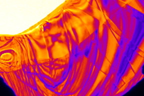 |
| This is a false-colored ultrafast electron microscope (UEM) snapshot of a thin semiconducting crystal. The image was captured with an extremely fast shutter lasting only a few hundred femtoseconds (a millionth of a billionth of a second).
Photo Credit: College of Science and Engineering |
Abstract:
Using a state-of-the-art ultrafast electron microscope, University of Minnesota researchers have recorded the first-ever videos showing how heat moves through materials at the nanoscale traveling at the speed of sound.
This video made with the University of Minnesota ultrafast electron microscope (UEM) shows the initial moments of thermal-energy motion in an imperfect semiconducting material. The video shows nanoscale waves of energy, called phonons, moving at about 6 nanometers (0.000000006 meters) per picosecond (0.000000000001 second).
Credit: College of Science and Engineering
First-ever videos show how heat moves through materials at the nanoscale and speed of sound: Groundbreaking observations could help develop better, more efficient materials for electronics and alternative energy
Minneapolis, MN | Posted on April 16th, 2016The research, published today in Nature Communications, provides unprecedented insight into roles played by individual atomic and nanoscale features that could aid in the design of better, more efficient materials with a wide array of uses, from personal electronics to alternative-energy technologies.
Energy in the form of heat impacts all technologies and is a major factor in how electronic devices and public infrastructure are designed and engineered. It is also the largest form of waste energy in critical applications, including power transmission and especially transportation, where, for example, roughly 70 percent of the energy in gasoline is wasted as heat in automobile engines.
Materials scientists and engineers have spent decades researching how to control thermal energy at the atomic level in order to recycle and use it to dramatically increase efficiencies and ultimately drive down the use of fossil fuels. Such work would be greatly aided by actually watching heat move through materials, but capturing images of the basic physical processes at the heart of thermal-energy motion has presented enormous challenges. This is because the fundamental length scales are nanometers (a billionth of a meter) and the speeds can be many miles per second. Such extreme conditions have made imaging this ubiquitous process extraordinarily challenging.
To overcome these challenges and image the movement of heat energy, the researchers used a cutting-edge FEI Tecnai� Femto ultrafast electron microscope (UEM) capable of examining the dynamics of materials at the atomic and molecular scale over time spans measured in femtoseconds (one millionth of a billionth of a second). In this work, the researchers used a brief laser pulse to excite electrons and very rapidly heat crystalline semiconducting materials of tungsten diselenide and germanium. They then captured slow-motion videos (slowed by over a billion times the normal speed) of the resulting waves of energy moving through the crystals.
"As soon as we saw the waves, we knew it was an extremely exciting observation," said lead researcher David Flannigan, an assistant professor of chemical engineering and materials science at the University of Minnesota. "Actually watching this process happen at the nanoscale is a dream come true."
Flannigan said the movement of heat through the material looks like ripples on a pond after a pebble is dropped in the water. The videos show waves of energy moving at about 6 nanometers (0.000000006 meters) per picosecond (0.000000000001 second). Mapping the oscillations of energy, called phonons, at the nanoscale is critical to developing a detailed understanding of the fundamentals of thermal-energy motion.
"In many applications, scientists and engineers want to understand thermal-energy motion, control it, collect it, and precisely guide it to do useful work or very quickly move it away from sensitive components," Flannigan said. "Because the lengths and times are so small and so fast, it has been very difficult to understand in detail how this occurs in materials that have imperfections, as essentially all materials do. Literally watching this process happen would go a very long way in building our understanding, and now we can do just that."
###
In addition to Flannigan, researchers involved in the study are University of Minnesota materials science graduate student Daniel R. Cremons and chemical engineering graduate student Dayne A. Plemmons. The research was funded primarily by the National Science Foundation through the University of Minnesota Materials Research Science and Engineering Center.
####
For more information, please click here
Contacts:
Rhonda Zurn
College of Science and Engineering
(612) 626-7959
Lacey Nygard
University News Service
(612) 625-0552
Copyright © University of Minnesota
If you have a comment, please Contact us.Issuers of news releases, not 7th Wave, Inc. or Nanotechnology Now, are solely responsible for the accuracy of the content.
Bookmark:


| Related Links |
| Related News Press |
News and information
![]() Quantum computer improves AI predictions April 17th, 2026
Quantum computer improves AI predictions April 17th, 2026
![]() Flexible sensor gains sensitivity under pressure April 17th, 2026
Flexible sensor gains sensitivity under pressure April 17th, 2026
![]() A reusable chip for particulate matter sensing April 17th, 2026
A reusable chip for particulate matter sensing April 17th, 2026
![]() Detecting vibrational quantum beating in the predissociation dynamics of SF6 using time-resolved photoelectron spectroscopy April 17th, 2026
Detecting vibrational quantum beating in the predissociation dynamics of SF6 using time-resolved photoelectron spectroscopy April 17th, 2026
Physics
![]() UC Irvine physicists discover method to reverse �quantum scrambling� : The work addresses the problem of information loss in quantum computing system April 17th, 2026
UC Irvine physicists discover method to reverse �quantum scrambling� : The work addresses the problem of information loss in quantum computing system April 17th, 2026
![]() Quantum computers simulate fundamental physics: shedding light on the building blocks of nature June 6th, 2025
Quantum computers simulate fundamental physics: shedding light on the building blocks of nature June 6th, 2025
Chemistry
![]() Projecting light to dispense liquids: A new route to ultra-precise microdroplets January 30th, 2026
Projecting light to dispense liquids: A new route to ultra-precise microdroplets January 30th, 2026
![]() From sensors to smart systems: the rise of AI-driven photonic noses January 30th, 2026
From sensors to smart systems: the rise of AI-driven photonic noses January 30th, 2026
![]() "Nanoreactor" cage uses visible light for catalytic and ultra-selective cross-cycloadditions October 3rd, 2025
"Nanoreactor" cage uses visible light for catalytic and ultra-selective cross-cycloadditions October 3rd, 2025
![]() Cambridge chemists discover simple way to build bigger molecules � one carbon at a time June 6th, 2025
Cambridge chemists discover simple way to build bigger molecules � one carbon at a time June 6th, 2025
Videos/Movies
![]() ICFO researchers overcome long-standing bottleneck in single photon detection with twisted 2D materials August 8th, 2025
ICFO researchers overcome long-standing bottleneck in single photon detection with twisted 2D materials August 8th, 2025
Govt.-Legislation/Regulation/Funding/Policy
![]() Quantum computer improves AI predictions April 17th, 2026
Quantum computer improves AI predictions April 17th, 2026
![]() Metasurfaces smooth light to boost magnetic sensing precision January 30th, 2026
Metasurfaces smooth light to boost magnetic sensing precision January 30th, 2026
![]() New imaging approach transforms study of bacterial biofilms August 8th, 2025
New imaging approach transforms study of bacterial biofilms August 8th, 2025
Discoveries
![]() Quantum computer improves AI predictions April 17th, 2026
Quantum computer improves AI predictions April 17th, 2026
![]() Flexible sensor gains sensitivity under pressure April 17th, 2026
Flexible sensor gains sensitivity under pressure April 17th, 2026
![]() A reusable chip for particulate matter sensing April 17th, 2026
A reusable chip for particulate matter sensing April 17th, 2026
![]() Detecting vibrational quantum beating in the predissociation dynamics of SF6 using time-resolved photoelectron spectroscopy April 17th, 2026
Detecting vibrational quantum beating in the predissociation dynamics of SF6 using time-resolved photoelectron spectroscopy April 17th, 2026
Materials/Metamaterials/Magnetoresistance
![]() First real-time observation of two-dimensional melting process: Researchers at Mainz University unveil new insights into magnetic vortex structures August 8th, 2025
First real-time observation of two-dimensional melting process: Researchers at Mainz University unveil new insights into magnetic vortex structures August 8th, 2025
![]() Researchers unveil a groundbreaking clay-based solution to capture carbon dioxide and combat climate change June 6th, 2025
Researchers unveil a groundbreaking clay-based solution to capture carbon dioxide and combat climate change June 6th, 2025
![]() A 1960s idea inspires NBI researchers to study hitherto inaccessible quantum states June 6th, 2025
A 1960s idea inspires NBI researchers to study hitherto inaccessible quantum states June 6th, 2025
![]() Institute for Nanoscience hosts annual proposal planning meeting May 16th, 2025
Institute for Nanoscience hosts annual proposal planning meeting May 16th, 2025
Announcements
![]() A fundamentally new therapeutic approach to cystic fibrosis: Nanobody repairs cellular defect April 17th, 2026
A fundamentally new therapeutic approach to cystic fibrosis: Nanobody repairs cellular defect April 17th, 2026
![]() UC Irvine physicists discover method to reverse �quantum scrambling� : The work addresses the problem of information loss in quantum computing system April 17th, 2026
UC Irvine physicists discover method to reverse �quantum scrambling� : The work addresses the problem of information loss in quantum computing system April 17th, 2026
Interviews/Book Reviews/Essays/Reports/Podcasts/Journals/White papers/Posters
![]() A fundamentally new therapeutic approach to cystic fibrosis: Nanobody repairs cellular defect April 17th, 2026
A fundamentally new therapeutic approach to cystic fibrosis: Nanobody repairs cellular defect April 17th, 2026
![]() UC Irvine physicists discover method to reverse �quantum scrambling� : The work addresses the problem of information loss in quantum computing system April 17th, 2026
UC Irvine physicists discover method to reverse �quantum scrambling� : The work addresses the problem of information loss in quantum computing system April 17th, 2026
Photonics/Optics/Lasers
![]() Metasurfaces smooth light to boost magnetic sensing precision January 30th, 2026
Metasurfaces smooth light to boost magnetic sensing precision January 30th, 2026
![]() From sensors to smart systems: the rise of AI-driven photonic noses January 30th, 2026
From sensors to smart systems: the rise of AI-driven photonic noses January 30th, 2026
|
|
||
|
|
||
| The latest news from around the world, FREE | ||
|
|
||
|
|
||
| Premium Products | ||
|
|
||
|
Only the news you want to read!
Learn More |
||
|
|
||
|
Full-service, expert consulting
Learn More |
||
|
|
||