Home > Press > IBS report electric transport across molybdenum disulfide grain boundaries: Scientific team from CINAP/IBS identifies previously undiscovered differences in grain boundaries
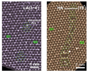 |
| Observing the location and angle of the GBs and the atomic structure. CREDIT: IBS |
Abstract:
The Center for Integrated Nanostructure Physics (CINAP) within IBS has reported results correlating the flake merging angle with grain boundary (GBs) properties, and proven that increasing the merging angle of GBs drastically improves the flow of electrons. This correlates to an increase in the carrier mobility from less than 1 cm2V-1s-1 for small angles, to 16cm2 V-1s-1 for angles greater than 20°. The paper, entitled, 'Misorientation-angle-dependent electrical transport across molybdenum disulfide grain boundaries' is published in the journal Nature Communications.
IBS report electric transport across molybdenum disulfide grain boundaries: Scientific team from CINAP/IBS identifies previously undiscovered differences in grain boundaries
Daejeon, Korea | Posted on January 28th, 2016According to the paper, it is essential to understand the atomic structures of GBs in order to control and improve electrical transport properties in both bulk and low-dimensional materials. Grain boundaries are the direction that atoms are arranged in a material. For the experiments undertaken by scientists at CINAP, a monolayer molybdenum disulfide (MoS2) was grown by chemical vapour deposition (CVD) and subsequently transferred to a substrate of silicon dioxide (SiO2). The team's reasoning for using MoS2 is twofold: firstly, it is a 2D semiconductor that features high electrical conductance and, crucially, has a natural bandgap, which enables it to be tuned on and off and; secondly, the grain boundaries are well-defined. This is paramount for successful experiments. Previous research from Northwestern University found that the GBs of MoS2 provided a unique way to modulate resistance; this was achieved by using a large electric field to spatially modulate the location of the grain boundaries.
The Northwestern results, published last year in Nature Nanotechnology, opened a pathway for future research, but the debate regarding the transport physics at the GB is still under dispute. This is due to a large device-to-device performance variation, poor single-domain carrier mobility, and, most importantly, a lack of correlation between transport properties and GB atomic structures in MoS2 research. The CINAP team, headed by the Center's director Young Hee Lee, overcame these obstacles by directly correlating four-probe transport measurements across single GBs with both high-resolution transmission electron microscopy (TEM) imaging and first-principles calculations. TEM is a microscopy technique whereby a beam of electrons is transmitted through an ultra-thin specimen, interacting with the specimen as it passes through. An exact atomic-scale image is formed from the interaction of the electrons transmitted through the specimen.
Identifying Grain Boundaries
GBs in the MoS2 layers were identified and regions with no sign of wrinkling or multilayers were then selected to prevent misinterpretations. Four-probe transport measurements were then performed on the substrate with surprising results; when measuring flake misorientations of 8-20o, mobility increased from much less than 1 cm2V-1s-1 up to 16cm2 V-1s-1. Above 20o field effect mobility saturates at a 16cm2 V-1s-1 intra-domain cutoff. Thus, GBs between flakes having a misorientation angle of 20-60o show better transport properties.
The team has, as reported in their paper, "provided a more unified picture of the relationship between mobility, merging angle and atomistic structures of the GBs of monolayer MoS2." The results provide practical expectations regarding transport properties in large-area films, which will be restricted largely by the poor mobility across GBs. The results obtained in this work are applicable to other similar 2D systems, and contribute to the fundamental understanding of transport in semiconductors.
####
For more information, please click here
Contacts:
Dahee Carol Kim
82-428-788-133
Copyright © Institute for Basic Science
If you have a comment, please Contact us.Issuers of news releases, not 7th Wave, Inc. or Nanotechnology Now, are solely responsible for the accuracy of the content.
Bookmark:


| Related Links |
| Related News Press |
News and information
![]() Quantum computer improves AI predictions April 17th, 2026
Quantum computer improves AI predictions April 17th, 2026
![]() Flexible sensor gains sensitivity under pressure April 17th, 2026
Flexible sensor gains sensitivity under pressure April 17th, 2026
![]() A reusable chip for particulate matter sensing April 17th, 2026
A reusable chip for particulate matter sensing April 17th, 2026
![]() Detecting vibrational quantum beating in the predissociation dynamics of SF6 using time-resolved photoelectron spectroscopy April 17th, 2026
Detecting vibrational quantum beating in the predissociation dynamics of SF6 using time-resolved photoelectron spectroscopy April 17th, 2026
Thin films
![]() Tiny nanosheets, big leap: A new sensor detects ethanol at ultra-low levels January 30th, 2026
Tiny nanosheets, big leap: A new sensor detects ethanol at ultra-low levels January 30th, 2026
![]() Utilizing palladium for addressing contact issues of buried oxide thin film transistors April 5th, 2024
Utilizing palladium for addressing contact issues of buried oxide thin film transistors April 5th, 2024
![]() Understanding the mechanism of non-uniform formation of diamond film on tools: Paving the way to a dry process with less environmental impact March 24th, 2023
Understanding the mechanism of non-uniform formation of diamond film on tools: Paving the way to a dry process with less environmental impact March 24th, 2023
![]() New study introduces the best graphite films: The work by Distinguished Professor Feng Ding at UNIST has been published in the October 2022 issue of Nature Nanotechnology November 4th, 2022
New study introduces the best graphite films: The work by Distinguished Professor Feng Ding at UNIST has been published in the October 2022 issue of Nature Nanotechnology November 4th, 2022
Chip Technology
![]() A reusable chip for particulate matter sensing April 17th, 2026
A reusable chip for particulate matter sensing April 17th, 2026
![]() Metasurfaces smooth light to boost magnetic sensing precision January 30th, 2026
Metasurfaces smooth light to boost magnetic sensing precision January 30th, 2026
Discoveries
![]() Quantum computer improves AI predictions April 17th, 2026
Quantum computer improves AI predictions April 17th, 2026
![]() Flexible sensor gains sensitivity under pressure April 17th, 2026
Flexible sensor gains sensitivity under pressure April 17th, 2026
![]() A reusable chip for particulate matter sensing April 17th, 2026
A reusable chip for particulate matter sensing April 17th, 2026
![]() Detecting vibrational quantum beating in the predissociation dynamics of SF6 using time-resolved photoelectron spectroscopy April 17th, 2026
Detecting vibrational quantum beating in the predissociation dynamics of SF6 using time-resolved photoelectron spectroscopy April 17th, 2026
Materials/Metamaterials/Magnetoresistance
![]() First real-time observation of two-dimensional melting process: Researchers at Mainz University unveil new insights into magnetic vortex structures August 8th, 2025
First real-time observation of two-dimensional melting process: Researchers at Mainz University unveil new insights into magnetic vortex structures August 8th, 2025
![]() Researchers unveil a groundbreaking clay-based solution to capture carbon dioxide and combat climate change June 6th, 2025
Researchers unveil a groundbreaking clay-based solution to capture carbon dioxide and combat climate change June 6th, 2025
![]() A 1960s idea inspires NBI researchers to study hitherto inaccessible quantum states June 6th, 2025
A 1960s idea inspires NBI researchers to study hitherto inaccessible quantum states June 6th, 2025
![]() Institute for Nanoscience hosts annual proposal planning meeting May 16th, 2025
Institute for Nanoscience hosts annual proposal planning meeting May 16th, 2025
Announcements
![]() A fundamentally new therapeutic approach to cystic fibrosis: Nanobody repairs cellular defect April 17th, 2026
A fundamentally new therapeutic approach to cystic fibrosis: Nanobody repairs cellular defect April 17th, 2026
![]() UC Irvine physicists discover method to reverse ‘quantum scrambling’ : The work addresses the problem of information loss in quantum computing system April 17th, 2026
UC Irvine physicists discover method to reverse ‘quantum scrambling’ : The work addresses the problem of information loss in quantum computing system April 17th, 2026
Interviews/Book Reviews/Essays/Reports/Podcasts/Journals/White papers/Posters
![]() A fundamentally new therapeutic approach to cystic fibrosis: Nanobody repairs cellular defect April 17th, 2026
A fundamentally new therapeutic approach to cystic fibrosis: Nanobody repairs cellular defect April 17th, 2026
![]() UC Irvine physicists discover method to reverse ‘quantum scrambling’ : The work addresses the problem of information loss in quantum computing system April 17th, 2026
UC Irvine physicists discover method to reverse ‘quantum scrambling’ : The work addresses the problem of information loss in quantum computing system April 17th, 2026
|
|
||
|
|
||
| The latest news from around the world, FREE | ||
|
|
||
|
|
||
| Premium Products | ||
|
|
||
|
Only the news you want to read!
Learn More |
||
|
|
||
|
Full-service, expert consulting
Learn More |
||
|
|
||