Home > Press > An Ultra-Bright and Highly Coherent Electron Source Developed to Improve the Performance of Electron-Beam Analytical Instrument
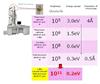 |
| Comparison between the recently developed LaB6 nanowire field-emission electron source and the conventional electron source. The use of the new electron emitter allowed the development of the source of ultra-bright electron beams, with their energy spread being two-thirds of the energy spread associated with a contemporary electron emitter. |
Abstract:
Researchers at the National Institute for Materials Science -- Han Zhang, Senior Researcher, Spin Characterization Group, and Jie Tang, Group Leader of the One-Dimensional Nanomaterials Group, Materials Processing Unit, and collaborators developed technology to fabricate lanthanum hexaboride (LaB6) single-crystal nanowires with clean surface, a promising cold field-emission electron source for electron microscopes and other devices, and thereby improved the performance and stability of the electron source. Furthermore, by installing the new electron source into a scanning electron microscope, they successfully obtained high-resolution images, demonstrating that the electron source can actually serve as a source of ultra-bright electron beams for electron microscopes.
An Ultra-Bright and Highly Coherent Electron Source Developed to Improve the Performance of Electron-Beam Analytical Instrument
Tsukuba, Japan | Posted on January 24th, 2016To increase the spatial resolution of electron microscopes, it is necessary to obtain ultra-bright and highly coherent electron beams by narrowly focusing a large amount of electrons emitted from an electron source. At present, high-resolution electron microscopes are equipped with needle-like tungsten as an electron source. To increase the spatial resolution of the microscope even higher, efforts had been made to develop a field emission electron source using LaB6, which emits electrons more easily than tungsten. However, the synthesis of nanowires -- a requirement for the development of a field emission electron source -- using LaB6 was challenging because this very hard material was difficult to handle.
In collaboration with Dr. Lu-Chang Qin, a professor at the University of North Carolina at Chapel Hill in the United States, the research team succeeded in the fabrication of the electron source consisting of a LaB6 nanowire by employing chemical vapor deposition. Furthermore, the research team developed technology to clean the surface of the LaB6 nanowire, which led to the improvement in electron emission characteristics and stability of the electron source. The research team confirmed that the newly developed LaB6 nanowire electron source was capable of producing highly coherent electron beams, which were 100 times brighter and had an energy spread of two-thirds compared to the current tungsten electron source. The team also verified that, when the electron source was installed in a field-emission electron microscope, its electron current density was 1,000 times greater than the conventional electron sources and it lasted 5 hours of use without attenuation in the emission current. Moreover, the team actually observed samples using an electron microscope equipped with the LaB6 nanowire electron source, and obtained electron microscopy images with a resolution higher than the conventional standard level.
The LaB6 nanowire electron source can be easily installed in devices by simply replacing the conventional tungsten electron gun (electron source) with it. In the future, the team plans to work on practical use and commercialization of the LaB6 nanowire electron source through joint research with industrial partners.
This research was carried out as a follow-up to the research project �Development of Next-Generation Electron Microscope Using Nanostructure-Controlled LaB6� (Jie Tang, Principal Investigator) conducted in the framework of Japan Science and Technology Agency�s program �Development of Advanced Measurement and Analysis Systems,� which aimed at the acceleration of innovation through industry-academia cooperation. This study was published in the online version of British scientific journal Nature Nanotechnology on November 30, 2015 (local time).
####
About National Institute for Materials Science (NIMS)
Public research institution for materials science in Japan.
For more information, please click here
Contacts:
Press Office
Jie Tang
Leader of the One-Dimensional Nanomaterials Group,
Materials Processing Unit, NIMS
Tel: +81-29-859-2728
Email: tang.jie=nims.go.jp
(Please replace �=� with
(Regarding public relations)
Public Relations Office
National Institute for Materials Science
1-2-1 Sengen, Tsukuba, Ibaraki, 305-0047, JAPAN
Tel: +81-29-859-2026, Fax: +81-29-859-2017
Email: pressrelease=ml.nims.go.jp
(Please replace �=� with
Copyright © AlphaGalileo
If you have a comment, please Contact us.Issuers of news releases, not 7th Wave, Inc. or Nanotechnology Now, are solely responsible for the accuracy of the content.
Bookmark:


| Related Links |
![]() Full bibliographic information
Full bibliographic information
| Related News Press |
News and information
![]() Quantum computer improves AI predictions April 17th, 2026
Quantum computer improves AI predictions April 17th, 2026
![]() Flexible sensor gains sensitivity under pressure April 17th, 2026
Flexible sensor gains sensitivity under pressure April 17th, 2026
![]() A reusable chip for particulate matter sensing April 17th, 2026
A reusable chip for particulate matter sensing April 17th, 2026
![]() Detecting vibrational quantum beating in the predissociation dynamics of SF6 using time-resolved photoelectron spectroscopy April 17th, 2026
Detecting vibrational quantum beating in the predissociation dynamics of SF6 using time-resolved photoelectron spectroscopy April 17th, 2026
Imaging
![]() Simple algorithm paired with standard imaging tool could predict failure in lithium metal batteries August 8th, 2025
Simple algorithm paired with standard imaging tool could predict failure in lithium metal batteries August 8th, 2025
Govt.-Legislation/Regulation/Funding/Policy
![]() Quantum computer improves AI predictions April 17th, 2026
Quantum computer improves AI predictions April 17th, 2026
![]() Metasurfaces smooth light to boost magnetic sensing precision January 30th, 2026
Metasurfaces smooth light to boost magnetic sensing precision January 30th, 2026
![]() New imaging approach transforms study of bacterial biofilms August 8th, 2025
New imaging approach transforms study of bacterial biofilms August 8th, 2025
Discoveries
![]() Quantum computer improves AI predictions April 17th, 2026
Quantum computer improves AI predictions April 17th, 2026
![]() Flexible sensor gains sensitivity under pressure April 17th, 2026
Flexible sensor gains sensitivity under pressure April 17th, 2026
![]() A reusable chip for particulate matter sensing April 17th, 2026
A reusable chip for particulate matter sensing April 17th, 2026
![]() Detecting vibrational quantum beating in the predissociation dynamics of SF6 using time-resolved photoelectron spectroscopy April 17th, 2026
Detecting vibrational quantum beating in the predissociation dynamics of SF6 using time-resolved photoelectron spectroscopy April 17th, 2026
Announcements
![]() A fundamentally new therapeutic approach to cystic fibrosis: Nanobody repairs cellular defect April 17th, 2026
A fundamentally new therapeutic approach to cystic fibrosis: Nanobody repairs cellular defect April 17th, 2026
![]() UC Irvine physicists discover method to reverse �quantum scrambling� : The work addresses the problem of information loss in quantum computing system April 17th, 2026
UC Irvine physicists discover method to reverse �quantum scrambling� : The work addresses the problem of information loss in quantum computing system April 17th, 2026
Interviews/Book Reviews/Essays/Reports/Podcasts/Journals/White papers/Posters
![]() A fundamentally new therapeutic approach to cystic fibrosis: Nanobody repairs cellular defect April 17th, 2026
A fundamentally new therapeutic approach to cystic fibrosis: Nanobody repairs cellular defect April 17th, 2026
![]() UC Irvine physicists discover method to reverse �quantum scrambling� : The work addresses the problem of information loss in quantum computing system April 17th, 2026
UC Irvine physicists discover method to reverse �quantum scrambling� : The work addresses the problem of information loss in quantum computing system April 17th, 2026
Tools
![]() Metasurfaces smooth light to boost magnetic sensing precision January 30th, 2026
Metasurfaces smooth light to boost magnetic sensing precision January 30th, 2026
![]() From sensors to smart systems: the rise of AI-driven photonic noses January 30th, 2026
From sensors to smart systems: the rise of AI-driven photonic noses January 30th, 2026
![]() Japan launches fully domestically produced quantum computer: Expo visitors to experience quantum computing firsthand August 8th, 2025
Japan launches fully domestically produced quantum computer: Expo visitors to experience quantum computing firsthand August 8th, 2025
|
|
||
|
|
||
| The latest news from around the world, FREE | ||
|
|
||
|
|
||
| Premium Products | ||
|
|
||
|
Only the news you want to read!
Learn More |
||
|
|
||
|
Full-service, expert consulting
Learn More |
||
|
|
||