Home > Press > CAMECA Helps US Navy LEAP Forward in Materials Design: CAMECA Delivers Local Electrode Atom Probe (LEAP) To US Naval Research Laboratory for Advanced Materials Development
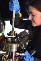 |
| The US Naval Research Laboratory (NRL) uses the CAMECA Local Electrode Atom Probe (LEAP) to provide nanoscale surface, bulk and interfacial materials analysis. Here a researcher loads a carousel of specimens into the LEAP for analysis. |
Abstract:
The US Naval Research Laboratory (NRL) has taken delivery of the US Department of Defense’s first Local Electrode Atom Probe (LEAP) microscope. The high- performance atom probe from CAMECA, a unit of AMETEK Materials Analysis, is used in advanced materials analysis to provide precise atom-by-atom identification, 3-D spatial positioning, and accurate atomic-scale reconstruction of a material’s microstructure. Since their development in the 1960s, atom probes have contributed to major advances in materials science.
CAMECA Helps US Navy LEAP Forward in Materials Design: CAMECA Delivers Local Electrode Atom Probe (LEAP) To US Naval Research Laboratory for Advanced Materials Development
Washington, DC | Posted on September 11th, 2015“The exact knowledge of where individual atoms are in a material is of tremendous benefit when engineering new materials,” notes Keith Knipling of the NRL Materials Science and Technology Division. “We expect the LEAP to greatly enhance our ability to develop new materials, including the next generation of structural alloys for stronger ship hulls and more advanced turbine engines, new electronic materials for tomorrow’s faster integrated circuits, and advanced solar cell and battery materials with improved power and energy efficiency.”
LEAP operates on the principle of field evaporation, whereby a strong electric field applied to a specimen is sufficient to cause removal of atoms by ionization. Proprietary single-particle detection enables isotopic identification by time-of-flight mass spectrometry and positional determination.
CAMECA’s LEAP system offers high data quality as well as improved ease of use via prefabricated MicrotipTM specimen carriers, which permit multiple samples to be prepared, mounted and loaded into the instrument for maximum efficiency for multi-experiment scenarios.
Atom evaporation is triggered either by a voltage or laser pulse applied to the sample. The resulting ions are accelerated away from the sample and identified. By repeating the sequence thousands of times per second, atoms are progressively removed from the sample tip and a 3D atomic-scale image of the material can be reconstructed.
“Mapping the location of each chemical species in a material microstructure enables an unprecedented understanding of the true effects of alloying and material synthesis, which is essentially for truly optimizing the properties of any material. We expect LEAP to deliver new atomic-scale perspectives and insights into a wide range of materials science investigations.”
Researchers at NRL, for example, are developing semiconductor materials with very dilute levels of added “dopant” atoms for the purpose of tailoring their electrical properties. These doped materials form the building blocks of nearly all semiconductor electronic devices, such as diodes, transistors, solar cells, light-emitting diodes and integrated circuits.
“Most analytical technical are incapable of measuring these low concentration levels, much less where the dopants are segregated within the microstructure. With LEAP, our researchers can now answer those questions,” adds Knipling.
CAMECA pioneered the development of atom probe tomography. Among its most recent advancements is the LEAP 5000, which sets the industry standard in terms of analytical accuracy, sensitivity, and 3D spatial resolution across a wide variety of metals, semiconductors and insulators and achieves an atom-by-atom identification efficiency of 80%.
####
About CAMECA
CAMECA® has more than 60 years of experience in the design, manufacture and servicing of scientific instruments for material micro- and nano-analysis. Since pioneering Electron Probe Microanalysis (EPMA) instrumentation in the 1950s and Secondary Ion Mass Spectrometry (SIMS) in the 1960s, CAMECA has remained an undisputed world leader, while achieving numerous breakthrough innovations in such complementary techniques as Low-energy Electron-induced X-ray Emission Spectrometry (LEXES) and Atom Probe Tomography (APT).
Headquartered near Paris, CAMECA also has a production facility in Madison WI, USA where the LEAP APT is designed and manufactured, further locations in Brazil, China, England, Germany, India, Japan, Korea, and Taiwan. CAMECA is a business unit of the Materials Analysis Division of AMETEK® Inc., a leading global manufacturer of electronic instruments and electromechanical products.
About the US Naval Research Laboratory
The US Naval Laboratory is the US Navy’s full-spectrum corporate laboratory, conducting a broadly based multidisciplinary program of scientific research and advanced technological development. The laboratory, which has served the US Navy for more than 90 years, continues to meet the complex technological challenges of today’s world. More information is available at www.nrl.navy
For more information, please click here
Contacts:
CAMECA LEAP Technology Ctr
AMETEK Materials Analysis
5500 Nobel Drive
Madison, WI 53711
Phone: +1 608-274-6880
Copyright © CAMECA
If you have a comment, please Contact us.Issuers of news releases, not 7th Wave, Inc. or Nanotechnology Now, are solely responsible for the accuracy of the content.
Bookmark:


| Related News Press |
News and information
![]() Quantum computer improves AI predictions April 17th, 2026
Quantum computer improves AI predictions April 17th, 2026
![]() Flexible sensor gains sensitivity under pressure April 17th, 2026
Flexible sensor gains sensitivity under pressure April 17th, 2026
![]() A reusable chip for particulate matter sensing April 17th, 2026
A reusable chip for particulate matter sensing April 17th, 2026
![]() Detecting vibrational quantum beating in the predissociation dynamics of SF6 using time-resolved photoelectron spectroscopy April 17th, 2026
Detecting vibrational quantum beating in the predissociation dynamics of SF6 using time-resolved photoelectron spectroscopy April 17th, 2026
Imaging
![]() Simple algorithm paired with standard imaging tool could predict failure in lithium metal batteries August 8th, 2025
Simple algorithm paired with standard imaging tool could predict failure in lithium metal batteries August 8th, 2025
![]() First real-time observation of two-dimensional melting process: Researchers at Mainz University unveil new insights into magnetic vortex structures August 8th, 2025
First real-time observation of two-dimensional melting process: Researchers at Mainz University unveil new insights into magnetic vortex structures August 8th, 2025
![]() New imaging approach transforms study of bacterial biofilms August 8th, 2025
New imaging approach transforms study of bacterial biofilms August 8th, 2025
Laboratories
![]() Researchers develop molecular qubits that communicate at telecom frequencies October 3rd, 2025
Researchers develop molecular qubits that communicate at telecom frequencies October 3rd, 2025
Govt.-Legislation/Regulation/Funding/Policy
![]() Quantum computer improves AI predictions April 17th, 2026
Quantum computer improves AI predictions April 17th, 2026
![]() Metasurfaces smooth light to boost magnetic sensing precision January 30th, 2026
Metasurfaces smooth light to boost magnetic sensing precision January 30th, 2026
![]() New imaging approach transforms study of bacterial biofilms August 8th, 2025
New imaging approach transforms study of bacterial biofilms August 8th, 2025
Announcements
![]() A fundamentally new therapeutic approach to cystic fibrosis: Nanobody repairs cellular defect April 17th, 2026
A fundamentally new therapeutic approach to cystic fibrosis: Nanobody repairs cellular defect April 17th, 2026
![]() UC Irvine physicists discover method to reverse ‘quantum scrambling’ : The work addresses the problem of information loss in quantum computing system April 17th, 2026
UC Irvine physicists discover method to reverse ‘quantum scrambling’ : The work addresses the problem of information loss in quantum computing system April 17th, 2026
Tools
![]() Metasurfaces smooth light to boost magnetic sensing precision January 30th, 2026
Metasurfaces smooth light to boost magnetic sensing precision January 30th, 2026
![]() From sensors to smart systems: the rise of AI-driven photonic noses January 30th, 2026
From sensors to smart systems: the rise of AI-driven photonic noses January 30th, 2026
![]() Japan launches fully domestically produced quantum computer: Expo visitors to experience quantum computing firsthand August 8th, 2025
Japan launches fully domestically produced quantum computer: Expo visitors to experience quantum computing firsthand August 8th, 2025
New-Contracts/Sales/Customers
![]() Bruker Light-Sheet Microscopes at Major Comprehensive Cancer Center: New Advanced Imaging Center Powered by Two MuVi and LCS SPIM Microscopes March 25th, 2021
Bruker Light-Sheet Microscopes at Major Comprehensive Cancer Center: New Advanced Imaging Center Powered by Two MuVi and LCS SPIM Microscopes March 25th, 2021
![]() Arrowhead Pharmaceuticals Announces Closing of Agreement with Takeda November 27th, 2020
Arrowhead Pharmaceuticals Announces Closing of Agreement with Takeda November 27th, 2020
![]() Veeco Announces Aledia Order of 300mm MOCVD Equipment for microLED Displays: Propel™ Platform First 300mm System with EFEM Designed for Advanced Display Applications October 20th, 2020
Veeco Announces Aledia Order of 300mm MOCVD Equipment for microLED Displays: Propel™ Platform First 300mm System with EFEM Designed for Advanced Display Applications October 20th, 2020
![]() GREENWAVES TECHNOLOGIES Announces Next Generation GAP9 Hearables Platform Using GLOBALFOUNDRIES 22FDX Solution October 16th, 2020
GREENWAVES TECHNOLOGIES Announces Next Generation GAP9 Hearables Platform Using GLOBALFOUNDRIES 22FDX Solution October 16th, 2020
|
|
||
|
|
||
| The latest news from around the world, FREE | ||
|
|
||
|
|
||
| Premium Products | ||
|
|
||
|
Only the news you want to read!
Learn More |
||
|
|
||
|
Full-service, expert consulting
Learn More |
||
|
|
||