Home > Press > JEOL Introduces New Best-in-Class Field Emission SEM
 |
Abstract:
JEOL USA has introduced a new entry-level, high-performance Field Emission Scanning Electron Microscope, demonstrated for the first time at M&M 2015 in Portland, Oregon.
JEOL Introduces New Best-in-Class Field Emission SEM
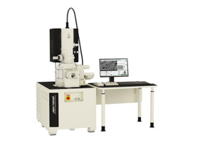
Peabody, MA | Posted on September 2nd, 2015The new JSM-7200F is a best-in-class FE SEM with ultrahigh spatial resolution of 1.6nm at 1.0kV and high probe current of 300nA. This versatile, user-friendly FE SEM is a compact system designed for easy installation and operation.
Featuring through-the-lens detectors that can collect a variety of signals by varying the built-in energy filter, the JSM-7200F produces a large amount of data in a very short amount of time. For the fast-paced manufacturing environment the JSM-7200F is a high throughput easy-to-use FE SEM. For the research environment, it offers the analyst a wide variety of contrast mechanisms. Seamless observation and analysis using EDS, WDS, EBSD, STEM, BSE, and CL can be conducted easily and efficiently.
The JSM-7200F is an all-in-one SEM designed for any type of sample or analysis, including magnetic samples, non-conducting materials, biological specimens, and semiconductor devices. It is the latest addition to JEOL's Field Emission SEM family, which includes the JSM-7800F PRIME with unmatched extreme high resolution and low and high kV (7� at both 1.0kV and 15kV) operation.
When integrated with Gatan 3View� Serial Block Face Imaging System, the JSM-7200F is ideal for neuroscience applications or any other 3D tomography imaging application.
A new Soft X-ray Emission Spectrometer designed for JEOL FE SEMs and microprobes allows efficient and parallel collection of very low energy-rays (WDS) with chemical state analysis.
The JSM-7200F offers the best resolution in its class for an entry level Field Emission SEM with a wide variety of analytical functions, fast acquisition with minimum beam dwell time, and a user-friendly interface for a multi-user environment with remote operation and diagnostics.
####
About JEOL USA
JEOL is a world leader in electron optical equipment and instrumentation for high-end scientific and industrial research and development. Core product groups include electron microscopes (SEMs and TEMs), instruments for the semiconductor industry (electron beam lithography and a series of defect review and inspection tools), and analytical instruments including mass spectrometers, NMRs and ESRs.
JEOL USA, Inc., a wholly owned subsidiary of JEOL, Ltd., Japan, was incorporated in the United States in 1962. The company has 13 regional service centers that offer unlimited emergency service and support in the U.S.
For more information, please click here
Contacts:
JEOL USA INC.
Pamela J. Mansfield
Marketing Communications
Direct: 978.536.2309
Copyright © JEOL USA
If you have a comment, please Contact us.Issuers of news releases, not 7th Wave, Inc. or Nanotechnology Now, are solely responsible for the accuracy of the content.
Bookmark:


| Related News Press |
News and information
![]() Quantum computer improves AI predictions April 17th, 2026
Quantum computer improves AI predictions April 17th, 2026
![]() Flexible sensor gains sensitivity under pressure April 17th, 2026
Flexible sensor gains sensitivity under pressure April 17th, 2026
![]() A reusable chip for particulate matter sensing April 17th, 2026
A reusable chip for particulate matter sensing April 17th, 2026
![]() Detecting vibrational quantum beating in the predissociation dynamics of SF6 using time-resolved photoelectron spectroscopy April 17th, 2026
Detecting vibrational quantum beating in the predissociation dynamics of SF6 using time-resolved photoelectron spectroscopy April 17th, 2026
Imaging
![]() Simple algorithm paired with standard imaging tool could predict failure in lithium metal batteries August 8th, 2025
Simple algorithm paired with standard imaging tool could predict failure in lithium metal batteries August 8th, 2025
Announcements
![]() A fundamentally new therapeutic approach to cystic fibrosis: Nanobody repairs cellular defect April 17th, 2026
A fundamentally new therapeutic approach to cystic fibrosis: Nanobody repairs cellular defect April 17th, 2026
![]() UC Irvine physicists discover method to reverse �quantum scrambling� : The work addresses the problem of information loss in quantum computing system April 17th, 2026
UC Irvine physicists discover method to reverse �quantum scrambling� : The work addresses the problem of information loss in quantum computing system April 17th, 2026
Tools
![]() Metasurfaces smooth light to boost magnetic sensing precision January 30th, 2026
Metasurfaces smooth light to boost magnetic sensing precision January 30th, 2026
![]() From sensors to smart systems: the rise of AI-driven photonic noses January 30th, 2026
From sensors to smart systems: the rise of AI-driven photonic noses January 30th, 2026
![]() Japan launches fully domestically produced quantum computer: Expo visitors to experience quantum computing firsthand August 8th, 2025
Japan launches fully domestically produced quantum computer: Expo visitors to experience quantum computing firsthand August 8th, 2025
Events/Classes
![]() Institute for Nanoscience hosts annual proposal planning meeting May 16th, 2025
Institute for Nanoscience hosts annual proposal planning meeting May 16th, 2025
![]() A New Blue: Mysterious origin of the ribbontail ray�s electric blue spots revealed July 5th, 2024
A New Blue: Mysterious origin of the ribbontail ray�s electric blue spots revealed July 5th, 2024
![]() Researchers demonstrate co-propagation of quantum and classical signals: Study shows that quantum encryption can be implemented in existing fiber networks January 20th, 2023
Researchers demonstrate co-propagation of quantum and classical signals: Study shows that quantum encryption can be implemented in existing fiber networks January 20th, 2023
|
|
||
|
|
||
| The latest news from around the world, FREE | ||
|
|
||
|
|
||
| Premium Products | ||
|
|
||
|
Only the news you want to read!
Learn More |
||
|
|
||
|
Full-service, expert consulting
Learn More |
||
|
|
||