Home > Press > Nanolab Technologies LEAPS Forward with High-Performance Analysis Services to the World: Nanolab Orders Advanced Local Electrode Atom Probe (LEAP®) Microscope from CAMECA Unit of AMETEK Materials Analysis Division
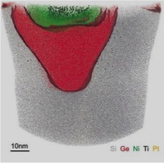 |
| Three-dimensional analysis of the source-drain region of a high-performance 28nm transistor revealing titanium and platinum doping in the nickel silicide to silicon germanium contact. Nanolab Technologies is the only analytical services company based in the United States providing such capability. |
Abstract:
Nanolab Technologies Inc., a Silicon Valley-based analytical services lab, has purchased a new Local Electrode Atom Probe from CAMECA Instruments Inc. The high-performance atom probe from CAMECA, a unit of the AMETEK Materials Analysis Division, is used to provide advanced materials analysis, including precise atom-by-atom identification, 3-D spatial positioning, and accurate atomic-scale reconstruction of a material’s microstructure.
Nanolab Technologies LEAPS Forward with High-Performance Analysis Services to the World: Nanolab Orders Advanced Local Electrode Atom Probe (LEAP®) Microscope from CAMECA Unit of AMETEK Materials Analysis Division
Milpitas, CA | Posted on August 27th, 2015Since their development in the 1960s, atom probes have contributed to major advances in materials science. Exclusively developed and manufactured by CAMECA, LEAP atom probes are used by the most prestigious research and development laboratories around the world, including seven of the ten largest computer chip manufacturers.
The LEAP system is the only technique available that provides three-dimensional sub- nanometer compositional information of all elements in a material. With its purchase of a LEAP instrument, Nanolab is set to become the only US- based analytical services company to offer this capability. Nanolab adds the LEAP to its already well-equipped laboratory with plans to offer LEAP analysis, concentrating on semiconductor failure analysis, process development and process control.
LEAP operates on the principle of field evaporation, whereby a strong electric field applied to a specimen is sufficient to cause removal of atoms by ionization. Proprietary single-particle detection enables isotopic identification by time-of-flight mass spectrometry as well as 3-D positional determination.
CAMECA’s LEAP system offers high data quality as well as improved ease of use via prefabricated MicrotipTM specimen carriers, which permit multiple samples to be prepared, mounted and loaded into the instrument for maximum efficiency for multi-experiment scenarios.
"Nanolab Technologies again has demonstrated its commitment to providing customers with access to state-of-the-art instruments critical to sustaining continued improvement in device performance," states John P. Traub, Nanolab President and Chief Executive Officer. "Our investment in new capabilities and technologies is unparalleled in analytical services and demonstrates the value Nanolab can deliver as a cost-effective alternative to insourcing. We expect our new CAMECA atom probe microscope to make valuable contributions to successfully solving our customers’ process and product development challenges."
####
About CAMECA
CAMECA® has more than 60 years of experience in the design, manufacture and servicing of scientific instruments for material micro- and nano-analysis. Since pioneering Electron Probe Microanalysis (EPMA) instrumentation in the 1950s and Secondary Ion Mass Spectrometry (SIMS) in the 1960s, CAMECA has remained an undisputed world leader, while achieving numerous breakthrough innovations in such complementary techniques as Low-energy Electron-induced X-ray Emission Spectrometry (LEXES) and Atom Probe Tomography (APT).
Headquartered near Paris, CAMECA also has a production facility in Madison WI, USA, where the LEAP atom probe is designed and manufactured as well as sales and service locations in Brazil, China, Germany, India, Japan, Korea, Taiwan and the United Kingdom. CAMECA is a business unit of the Materials Analysis Division of AMETEK Inc., a leading global manufacturer of electronic instruments and electromechanical devices.
About Nanolab Technologies
Nanolab Technologies provides knowledge-based analytical services, including advanced microscopy, chemical analysis, electrical failure analysis, materials analysis, FIB circuit edit, and defect analysis to the semiconductor, solar, MEMS, LED, medical device and other high- technologies industries. A private, employee-owned company, Nanolab Technologies designed and occupies a 48,000-square-foot, advanced laboratory in California’s Silicon Valley that utilizes leading-edge, extreme high-spatial-resolution instruments to meet the requirements of current and future technology nodes. It has a second facility located at the College of Nanoscale Science and Engineering (CNSE) at the University of Albany. For more information, visit www.nanolabtechnologies.com
For more information, please click here
Contacts:
John Traub
(Nanolab Technologies)
Telephone: +1-408-433-3320
Marion Chopin
(CAMECA SAS):
Telephone: +33 1 4334 6250
Copyright © CAMECA
If you have a comment, please Contact us.Issuers of news releases, not 7th Wave, Inc. or Nanotechnology Now, are solely responsible for the accuracy of the content.
Bookmark:


| Related News Press |
News and information
![]() Quantum computer improves AI predictions April 17th, 2026
Quantum computer improves AI predictions April 17th, 2026
![]() Flexible sensor gains sensitivity under pressure April 17th, 2026
Flexible sensor gains sensitivity under pressure April 17th, 2026
![]() A reusable chip for particulate matter sensing April 17th, 2026
A reusable chip for particulate matter sensing April 17th, 2026
![]() Detecting vibrational quantum beating in the predissociation dynamics of SF6 using time-resolved photoelectron spectroscopy April 17th, 2026
Detecting vibrational quantum beating in the predissociation dynamics of SF6 using time-resolved photoelectron spectroscopy April 17th, 2026
Imaging
![]() Simple algorithm paired with standard imaging tool could predict failure in lithium metal batteries August 8th, 2025
Simple algorithm paired with standard imaging tool could predict failure in lithium metal batteries August 8th, 2025
Announcements
![]() A fundamentally new therapeutic approach to cystic fibrosis: Nanobody repairs cellular defect April 17th, 2026
A fundamentally new therapeutic approach to cystic fibrosis: Nanobody repairs cellular defect April 17th, 2026
![]() UC Irvine physicists discover method to reverse ‘quantum scrambling’ : The work addresses the problem of information loss in quantum computing system April 17th, 2026
UC Irvine physicists discover method to reverse ‘quantum scrambling’ : The work addresses the problem of information loss in quantum computing system April 17th, 2026
Tools
![]() Metasurfaces smooth light to boost magnetic sensing precision January 30th, 2026
Metasurfaces smooth light to boost magnetic sensing precision January 30th, 2026
![]() From sensors to smart systems: the rise of AI-driven photonic noses January 30th, 2026
From sensors to smart systems: the rise of AI-driven photonic noses January 30th, 2026
![]() Japan launches fully domestically produced quantum computer: Expo visitors to experience quantum computing firsthand August 8th, 2025
Japan launches fully domestically produced quantum computer: Expo visitors to experience quantum computing firsthand August 8th, 2025
New-Contracts/Sales/Customers
![]() Bruker Light-Sheet Microscopes at Major Comprehensive Cancer Center: New Advanced Imaging Center Powered by Two MuVi and LCS SPIM Microscopes March 25th, 2021
Bruker Light-Sheet Microscopes at Major Comprehensive Cancer Center: New Advanced Imaging Center Powered by Two MuVi and LCS SPIM Microscopes March 25th, 2021
![]() Arrowhead Pharmaceuticals Announces Closing of Agreement with Takeda November 27th, 2020
Arrowhead Pharmaceuticals Announces Closing of Agreement with Takeda November 27th, 2020
![]() Veeco Announces Aledia Order of 300mm MOCVD Equipment for microLED Displays: Propel™ Platform First 300mm System with EFEM Designed for Advanced Display Applications October 20th, 2020
Veeco Announces Aledia Order of 300mm MOCVD Equipment for microLED Displays: Propel™ Platform First 300mm System with EFEM Designed for Advanced Display Applications October 20th, 2020
![]() GREENWAVES TECHNOLOGIES Announces Next Generation GAP9 Hearables Platform Using GLOBALFOUNDRIES 22FDX Solution October 16th, 2020
GREENWAVES TECHNOLOGIES Announces Next Generation GAP9 Hearables Platform Using GLOBALFOUNDRIES 22FDX Solution October 16th, 2020
|
|
||
|
|
||
| The latest news from around the world, FREE | ||
|
|
||
|
|
||
| Premium Products | ||
|
|
||
|
Only the news you want to read!
Learn More |
||
|
|
||
|
Full-service, expert consulting
Learn More |
||
|
|
||