Home > Press > Short wavelength plasmons observed in nanotubes: Berkeley Lab researchers create Ludinger liquid plasmons in metallic SWNTs
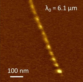 |
| This s-SNOM infrared image shows Luttinger-liquid plasmons in a metallic single-walled nanotube. CREDIT: Courtesy of Feng Wang, Berkeley Lab |
Abstract:
The term "plasmons" might sound like something from the soon-to-be-released new Star Wars movie, but the effects of plasmons have been known about for centuries. Plasmons are collective oscillations of conduction electrons (those loosely attached to molecules and atoms) that roll across the surfaces of metals while interacting with photons. For example, plasmons from nanoparticles of gold, silver and other metals interact with visible light photons to generate the vibrant colors displayed by stained glass, a technology that dates back more than 1,000 years. But plasmons have high-technology applications as well. In fact, there's even an emerging technology named for them - plasmonics - that holds great promise for superfast computers and optical microscopy.
Short wavelength plasmons observed in nanotubes: Berkeley Lab researchers create Ludinger liquid plasmons in metallic SWNTs
Berkeley, CA | Posted on July 28th, 2015At the heart of the high-technology applications of plasmons is their unique ability to confine the energy of a photon into a spatial dimension smaller than the photon's wavelength. Now, a team of researchers with Berkeley Lab's Materials Sciences Division, working at the Advanced Light Source (ALS), has generated and detected plasmons that boast one of the strongest confinement factors ever: the plasmon wavelength is only one hundredth of the free-space photon wavelength.
By focusing infrared light onto the tip of an Atomic Force Microscope, the researchers were able to observe what are called "Luttinger-liquid" plasmons in metallic single-walled nanotubes. A Luttinger-liquid is the theory that describes the flow of electrons through one-dimensional objects, such as a single-walled nanotube (SWNT), much as the Fermi-liquid theory describes the flow of electrons through most two- and three-dimensional metals.
"It is amazing that a plasmon in an individual nanotube, a 1-D object barely a single nanometer in diameter, can even be observed at all," says Feng Wang, a condensed matter physicist with Berkeley Lab's Materials Sciences Division who led this work. "Our use of scattering-type scanning near-field optical microscopy (s-SNOM) is enabling us to study Luttinger-liquid physics and explore novel plasmonic devices with extraordinary sub-wavelength confinement, almost 100 million times smaller in volume than that of free-space photons. What we're observing could hold great promise for novel plasmonic and nanophotonic devices over a broad frequency range, including telecom wavelengths."
Wang, who also holds appointments with the University California (UC) Berkeley Physics Department and the Kavli Energy NanoScience Institute (Kavli-ENSI), is the corresponding author of a paper in Nature Photonics that describes this research. The paper is titled "Observation of a Luttinger-liquid plasmon in metallic single-walled carbon nanotubes." The co-lead authors are Zhiwen Shi and Xiaoping Hong, both members of Wang's UC Berkeley research group. Other co-authors are Hans Bechtel, Bo Zeng, Michael Martin, Kenji Watanabe, Takashi Taniguchi and Yuen-Ron Shen.
Despite the enormous potential of plasmons for the integration of nanoscale photonics and electronics, the development of nanophotonic circuits based on classical plasmons has been significantly hampered by the difficulty in achieving broadband plasmonic waveguides that simultaneously exhibit strong spatial confinement, a high quality factor and low dispersion. The observations of Wang and his colleagues demonstrate that Luttinger-liquid plasmon of 1-D conduction electrons in SWNTs behaves much differently from classical plasmons.
"Luttinger-liquid plasmons in SWNTs propagate at semi-quantized velocities that are independent of carrier concentration or excitation wavelength, and simultaneously exhibit extraordinary spatial confinement, a high quality factor and low dispersion," says co-lead author Shi. "Usually, to be manipulated efficiently with a photonic device, the light wavelength is required to be smaller than the device. By concentrating photon energy at deep sub-wavelength scales, Luttinger-liquid plasmons in SWNTs effectively reduce the light wavelength. This should allow for the miniaturization of photonic devices down to the nanometer scale."
Wang, Shi, Hong and their colleagues observed Luttinger-liquid plasmons using the s-SNOM setup at ALS Beamline 5.4.1. Metallic SWNTs with diameters ranging from 1.2 to 1.7 nanometers were grown, purified and then deposited on a boron nitride substrate. Single wavelength infrared light was focused onto the tip of an Atomic Force Microscope to excite and detect a plasmon wave along an SWNT.
"Our direct observation of Luttinger-liquid plasmons opens up exciting new opportunities," Wang says. "For example, we're now exploring these plasmons in telecom wavelengths, the most widely used in photonics and integrated optics. We're also learning how the properties of these plasmons might be manipulated through electrostatic gating, mechanical strain and external magnetic fields."
###
This research was primarily supported by the U.S. Department of Energy's Office of Science.
####
About DOE/Lawrence Berkeley National Laboratory
Lawrence Berkeley National Laboratory addresses the world's most urgent scientific challenges by advancing sustainable energy, protecting human health, creating new materials, and revealing the origin and fate of the universe. Founded in 1931, Berkeley Lab's scientific expertise has been recognized with 13 Nobel prizes. The University of California manages Berkeley Lab for the U.S. Department of Energy's Office of Science. For more, visit www.lbl.gov.
DOE's Office of Science is the single largest supporter of basic research in the physical sciences in the United States, and is working to address some of the most pressing challenges of our time. For more information, please visit the Office of Science website at science.energy.gov/.
For more information, please click here
Contacts:
Lynn Yarris
510-486-5375
Copyright © DOE/Lawrence Berkeley National Laboratory
If you have a comment, please Contact us.Issuers of news releases, not 7th Wave, Inc. or Nanotechnology Now, are solely responsible for the accuracy of the content.
Bookmark:


| Related News Press |
News and information
![]() Quantum computer improves AI predictions April 17th, 2026
Quantum computer improves AI predictions April 17th, 2026
![]() Flexible sensor gains sensitivity under pressure April 17th, 2026
Flexible sensor gains sensitivity under pressure April 17th, 2026
![]() A reusable chip for particulate matter sensing April 17th, 2026
A reusable chip for particulate matter sensing April 17th, 2026
![]() Detecting vibrational quantum beating in the predissociation dynamics of SF6 using time-resolved photoelectron spectroscopy April 17th, 2026
Detecting vibrational quantum beating in the predissociation dynamics of SF6 using time-resolved photoelectron spectroscopy April 17th, 2026
Imaging
![]() Simple algorithm paired with standard imaging tool could predict failure in lithium metal batteries August 8th, 2025
Simple algorithm paired with standard imaging tool could predict failure in lithium metal batteries August 8th, 2025
![]() First real-time observation of two-dimensional melting process: Researchers at Mainz University unveil new insights into magnetic vortex structures August 8th, 2025
First real-time observation of two-dimensional melting process: Researchers at Mainz University unveil new insights into magnetic vortex structures August 8th, 2025
![]() New imaging approach transforms study of bacterial biofilms August 8th, 2025
New imaging approach transforms study of bacterial biofilms August 8th, 2025
Laboratories
![]() Researchers develop molecular qubits that communicate at telecom frequencies October 3rd, 2025
Researchers develop molecular qubits that communicate at telecom frequencies October 3rd, 2025
Govt.-Legislation/Regulation/Funding/Policy
![]() Quantum computer improves AI predictions April 17th, 2026
Quantum computer improves AI predictions April 17th, 2026
![]() Metasurfaces smooth light to boost magnetic sensing precision January 30th, 2026
Metasurfaces smooth light to boost magnetic sensing precision January 30th, 2026
![]() New imaging approach transforms study of bacterial biofilms August 8th, 2025
New imaging approach transforms study of bacterial biofilms August 8th, 2025
Chip Technology
![]() A reusable chip for particulate matter sensing April 17th, 2026
A reusable chip for particulate matter sensing April 17th, 2026
![]() Metasurfaces smooth light to boost magnetic sensing precision January 30th, 2026
Metasurfaces smooth light to boost magnetic sensing precision January 30th, 2026
Nanotubes/Buckyballs/Fullerenes/Nanorods/Nanostrings/Nanosheets
![]() Tiny nanosheets, big leap: A new sensor detects ethanol at ultra-low levels January 30th, 2026
Tiny nanosheets, big leap: A new sensor detects ethanol at ultra-low levels January 30th, 2026
![]() Enhancing power factor of p- and n-type single-walled carbon nanotubes April 25th, 2025
Enhancing power factor of p- and n-type single-walled carbon nanotubes April 25th, 2025
![]() Chainmail-like material could be the future of armor: First 2D mechanically interlocked polymer exhibits exceptional flexibility and strength January 17th, 2025
Chainmail-like material could be the future of armor: First 2D mechanically interlocked polymer exhibits exceptional flexibility and strength January 17th, 2025
![]() Innovative biomimetic superhydrophobic coating combines repair and buffering properties for superior anti-erosion December 13th, 2024
Innovative biomimetic superhydrophobic coating combines repair and buffering properties for superior anti-erosion December 13th, 2024
Optical computing/Photonic computing
![]() ICFO researchers overcome long-standing bottleneck in single photon detection with twisted 2D materials August 8th, 2025
ICFO researchers overcome long-standing bottleneck in single photon detection with twisted 2D materials August 8th, 2025
![]() Programmable electron-induced color router array May 14th, 2025
Programmable electron-induced color router array May 14th, 2025
Discoveries
![]() Quantum computer improves AI predictions April 17th, 2026
Quantum computer improves AI predictions April 17th, 2026
![]() Flexible sensor gains sensitivity under pressure April 17th, 2026
Flexible sensor gains sensitivity under pressure April 17th, 2026
![]() A reusable chip for particulate matter sensing April 17th, 2026
A reusable chip for particulate matter sensing April 17th, 2026
![]() Detecting vibrational quantum beating in the predissociation dynamics of SF6 using time-resolved photoelectron spectroscopy April 17th, 2026
Detecting vibrational quantum beating in the predissociation dynamics of SF6 using time-resolved photoelectron spectroscopy April 17th, 2026
Announcements
![]() A fundamentally new therapeutic approach to cystic fibrosis: Nanobody repairs cellular defect April 17th, 2026
A fundamentally new therapeutic approach to cystic fibrosis: Nanobody repairs cellular defect April 17th, 2026
![]() UC Irvine physicists discover method to reverse �quantum scrambling� : The work addresses the problem of information loss in quantum computing system April 17th, 2026
UC Irvine physicists discover method to reverse �quantum scrambling� : The work addresses the problem of information loss in quantum computing system April 17th, 2026
Interviews/Book Reviews/Essays/Reports/Podcasts/Journals/White papers/Posters
![]() A fundamentally new therapeutic approach to cystic fibrosis: Nanobody repairs cellular defect April 17th, 2026
A fundamentally new therapeutic approach to cystic fibrosis: Nanobody repairs cellular defect April 17th, 2026
![]() UC Irvine physicists discover method to reverse �quantum scrambling� : The work addresses the problem of information loss in quantum computing system April 17th, 2026
UC Irvine physicists discover method to reverse �quantum scrambling� : The work addresses the problem of information loss in quantum computing system April 17th, 2026
Photonics/Optics/Lasers
![]() Metasurfaces smooth light to boost magnetic sensing precision January 30th, 2026
Metasurfaces smooth light to boost magnetic sensing precision January 30th, 2026
![]() From sensors to smart systems: the rise of AI-driven photonic noses January 30th, 2026
From sensors to smart systems: the rise of AI-driven photonic noses January 30th, 2026
|
|
||
|
|
||
| The latest news from around the world, FREE | ||
|
|
||
|
|
||
| Premium Products | ||
|
|
||
|
Only the news you want to read!
Learn More |
||
|
|
||
|
Full-service, expert consulting
Learn More |
||
|
|
||