Home > Press > Could black phosphorus be the next silicon? New material could make it possible to pack more transistors on a chip, research suggests
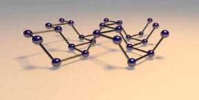 |
| This is a schematic of the "puckered honeycomb" crystal structure of black phosphorus. CREDIT: Vahid Tayari/McGill University |
Abstract:
As scientists continue to hunt for a material that will make it possible to pack more transistors on a chip, new research from McGill University and Université de Montréal adds to evidence that black phosphorus could emerge as a strong candidate.
Could black phosphorus be the next silicon? New material could make it possible to pack more transistors on a chip, research suggests
Montreal, Canada | Posted on July 7th, 2015In a study published today in Nature Communications, the researchers report that when electrons move in a phosphorus transistor, they do so only in two dimensions. The finding suggests that black phosphorus could help engineers surmount one of the big challenges for future electronics: designing energy-efficient transistors.
"Transistors work more efficiently when they are thin, with electrons moving in only two dimensions," says Thomas Szkopek, an associate professor in McGill's Department of Electrical and Computer Engineering and senior author of the new study. "Nothing gets thinner than a single layer of atoms."
In 2004, physicists at the University of Manchester in the U.K. first isolated and explored the remarkable properties of graphene -- a one-atom-thick layer of carbon. Since then scientists have rushed to to investigate a range of other two-dimensional materials. One of those is black phosphorus, a form of phosphorus that is similar to graphite and can be separated easily into single atomic layers, known as phosphorene.
Phosphorene has sparked growing interest because it overcomes many of the challenges of using graphene in electronics. Unlike graphene, which acts like a metal, black phosphorus is a natural semiconductor: it can be readily switched on and off.
"To lower the operating voltage of transistors, and thereby reduce the heat they generate, we have to get closer and closer to designing the transistor at the atomic level," Szkopek says. "The toolbox of the future for transistor designers will require a variety of atomic-layered materials: an ideal semiconductor, an ideal metal, and an ideal dielectric. All three components must be optimized for a well designed transistor. Black phosphorus fills the semiconducting-material role."
The work resulted from a multidisciplinary collaboration among Szkopek's nanoelectronics research group, the nanoscience lab of McGill Physics Prof. Guillaume Gervais, and the nanostructures research group of Prof. Richard Martel in Université de Montréal's Department of Chemistry.
To examine how the electrons move in a phosphorus transistor, the researchers observed them under the influence of a magnetic field in experiments performed at the National High Magnetic Field Laboratory in Tallahassee, FL, the largest and highest-powered magnet laboratory in the world. This research "provides important insights into the fundamental physics that dictate the behavior of black phosphorus," says Tim Murphy, DC Field Facility Director at the Florida facility.
"What's surprising in these results is that the electrons are able to be pulled into a sheet of charge which is two-dimensional, even though they occupy a volume that is several atomic layers in thickness," Szkopek says. That finding is significant because it could potentially facilitate manufacturing the material -- though at this point "no one knows how to manufacture this material on a large scale."
"There is a great emerging interest around the world in black phosphorus," Szkopek says. "We are still a long way from seeing atomic layer transistors in a commercial product, but we have now moved one step closer."
###
This work was funded by the Natural Sciences and Engineering Research Council of Canada, the Canadian Institute for Advanced Research, the Fonds de recherche du Québec - Nature et technologies, Le regroupement québécois sur les matériaux de pointe, and the Canada Research Chairs program. A portion of the work was performed at the National High Magnetic Field Laboratory which is supported by the National Science Foundation, the State of Florida and the U.S. Department of Energy.
"Two-dimensional magnetotransport in a black phosphorus naked quantum well", V. Tayari et al, published online in Nature Communications, July 7, 2015. DOI: 10.1038/ncomms8702
####
For more information, please click here
Contacts:
Chris Chipello
514-398-4201
http://www.mcgill.ca/newsroom/
http://twitter.com/McGilluMedia
Prof. Thomas Szkopek
Dept of Electrical and Computer Engineering
McGill University
William Raillant-Clark
International Press Attaché
Université de Montréal
Tel.: 514 343-7593
Copyright © McGill University
If you have a comment, please Contact us.Issuers of news releases, not 7th Wave, Inc. or Nanotechnology Now, are solely responsible for the accuracy of the content.
Bookmark:


| Related News Press |
News and information
![]() Quantum computer improves AI predictions April 17th, 2026
Quantum computer improves AI predictions April 17th, 2026
![]() Flexible sensor gains sensitivity under pressure April 17th, 2026
Flexible sensor gains sensitivity under pressure April 17th, 2026
![]() A reusable chip for particulate matter sensing April 17th, 2026
A reusable chip for particulate matter sensing April 17th, 2026
![]() Detecting vibrational quantum beating in the predissociation dynamics of SF6 using time-resolved photoelectron spectroscopy April 17th, 2026
Detecting vibrational quantum beating in the predissociation dynamics of SF6 using time-resolved photoelectron spectroscopy April 17th, 2026
Physics
![]() UC Irvine physicists discover method to reverse ‘quantum scrambling’ : The work addresses the problem of information loss in quantum computing system April 17th, 2026
UC Irvine physicists discover method to reverse ‘quantum scrambling’ : The work addresses the problem of information loss in quantum computing system April 17th, 2026
![]() Quantum computers simulate fundamental physics: shedding light on the building blocks of nature June 6th, 2025
Quantum computers simulate fundamental physics: shedding light on the building blocks of nature June 6th, 2025
![]() A 1960s idea inspires NBI researchers to study hitherto inaccessible quantum states June 6th, 2025
A 1960s idea inspires NBI researchers to study hitherto inaccessible quantum states June 6th, 2025
![]() Magnetism in new exotic material opens the way for robust quantum computers June 4th, 2025
Magnetism in new exotic material opens the way for robust quantum computers June 4th, 2025
Laboratories
![]() Researchers develop molecular qubits that communicate at telecom frequencies October 3rd, 2025
Researchers develop molecular qubits that communicate at telecom frequencies October 3rd, 2025
Graphene/ Graphite
![]() Electrifying results shed light on graphene foam as a potential material for lab grown cartilage June 6th, 2025
Electrifying results shed light on graphene foam as a potential material for lab grown cartilage June 6th, 2025
Govt.-Legislation/Regulation/Funding/Policy
![]() Quantum computer improves AI predictions April 17th, 2026
Quantum computer improves AI predictions April 17th, 2026
![]() Metasurfaces smooth light to boost magnetic sensing precision January 30th, 2026
Metasurfaces smooth light to boost magnetic sensing precision January 30th, 2026
![]() New imaging approach transforms study of bacterial biofilms August 8th, 2025
New imaging approach transforms study of bacterial biofilms August 8th, 2025
Chip Technology
![]() A reusable chip for particulate matter sensing April 17th, 2026
A reusable chip for particulate matter sensing April 17th, 2026
![]() Metasurfaces smooth light to boost magnetic sensing precision January 30th, 2026
Metasurfaces smooth light to boost magnetic sensing precision January 30th, 2026
Discoveries
![]() Quantum computer improves AI predictions April 17th, 2026
Quantum computer improves AI predictions April 17th, 2026
![]() Flexible sensor gains sensitivity under pressure April 17th, 2026
Flexible sensor gains sensitivity under pressure April 17th, 2026
![]() A reusable chip for particulate matter sensing April 17th, 2026
A reusable chip for particulate matter sensing April 17th, 2026
![]() Detecting vibrational quantum beating in the predissociation dynamics of SF6 using time-resolved photoelectron spectroscopy April 17th, 2026
Detecting vibrational quantum beating in the predissociation dynamics of SF6 using time-resolved photoelectron spectroscopy April 17th, 2026
Announcements
![]() A fundamentally new therapeutic approach to cystic fibrosis: Nanobody repairs cellular defect April 17th, 2026
A fundamentally new therapeutic approach to cystic fibrosis: Nanobody repairs cellular defect April 17th, 2026
![]() UC Irvine physicists discover method to reverse ‘quantum scrambling’ : The work addresses the problem of information loss in quantum computing system April 17th, 2026
UC Irvine physicists discover method to reverse ‘quantum scrambling’ : The work addresses the problem of information loss in quantum computing system April 17th, 2026
Interviews/Book Reviews/Essays/Reports/Podcasts/Journals/White papers/Posters
![]() A fundamentally new therapeutic approach to cystic fibrosis: Nanobody repairs cellular defect April 17th, 2026
A fundamentally new therapeutic approach to cystic fibrosis: Nanobody repairs cellular defect April 17th, 2026
![]() UC Irvine physicists discover method to reverse ‘quantum scrambling’ : The work addresses the problem of information loss in quantum computing system April 17th, 2026
UC Irvine physicists discover method to reverse ‘quantum scrambling’ : The work addresses the problem of information loss in quantum computing system April 17th, 2026
|
|
||
|
|
||
| The latest news from around the world, FREE | ||
|
|
||
|
|
||
| Premium Products | ||
|
|
||
|
Only the news you want to read!
Learn More |
||
|
|
||
|
Full-service, expert consulting
Learn More |
||
|
|
||