Home > Press > The microscopic topography of ink on paper: Researchers have analyzed the varying thickness of printed toner in unprecedented 3-D detail, yielding insights that could lead to higher quality, less expensive and more environmentally-friendly glossy and non-glossy papers
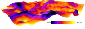 |
| This image shows a 3-D visualization of the toner layer on top of coated paper. The dark blue areas show thin layers of toner, whereas the yellow shows thicker layers. CREDIT:Markko Myllys/University of Jyvaskyla |
Abstract:
A team of Finnish scientists has found a new way to examine the ancient art of putting ink to paper in unprecedented 3-D detail. The technique could improve scientists' understanding of how ink sticks to paper and ultimately lead to higher quality, less expensive and more environmentally-friendly printed products.
The microscopic topography of ink on paper: Researchers have analyzed the varying thickness of printed toner in unprecedented 3-D detail, yielding insights that could lead to higher quality, less expensive and more environmentally-friendly glossy and non-glossy papers
Washington, DC | Posted on April 14th, 2015Using modern X-ray and laser-based technologies, the researchers created a nano-scale map of the varying thickness of toner ink on paper. They discovered that wood fibers protruding from the paper received relatively thin coatings of ink. In general, they also found the toner thickness was dictated mainly by the local changes in roughness, rather than the chemical variations caused by the paper's uneven glossy finish.
The team describes their results in a paper published in the Journal of Applied Physics, from AIP Publishing.
"We believe that this gives new insight, especially on how the topography of paper impacts the ink setting or consolidation," said Markko Myllys, an applied physicist at the University of Jyvaskyla in Finland. "This in turn helps us understand how glossy and non-glossy printed surfaces should be made."
Intricate Ink and Paper Microstructures
To achieve their detailed picture of ink thickness, the researchers first examined the underlying paper with X-ray microtomography, a smaller cousin of the CT scanning technology used in hospitals to produce images of the inside of the body.
To analyze the cyan ink layers, the researchers used two additional technologies: optical profilometry, which bounced a light beam off the surface of the ink to obtain a surface profile, and laser ablation, which zapped away controlled amounts of ink with a laser to determine the ink depth.
Although none of the imaging techniques are themselves new, the researchers were the first to combine all three to achieve a complete, high-resolution 3-D image of the intricate ink and paper microstructures.
The final images resemble a rugged mountain landscape, with the higher peaks generally showing thinner coatings of ink, and the valleys showing thicker pools.
The researchers found the typical ink layer was approximately 2.5 micrometers deep, about 1/40 the thickness of an average sheet of paper, but with relatively large spatial variations between the thickest and thinnest areas.
Knowing how topographical variations affect ink thickness will help the printing industry create more environmentally-friendly and less energy-demanding ink and optimize the size distribution of ink particles, Myllys said. It could also help the papermaking industry design more sustainable paper and packaging, for example from recycled components, while still maintaining the quality needed to make ink stick well. Additionally, the papermaking industry could use the findings to help decide how best to incorporate smart and novel features into paper, Myllys said.
The team believes the imaging methods they used can also be adapted to effectively analyze the thickness variations in other types of thin films, including those found in microelectronics, wear-resistant coatings and solar panels.
"This result can certainly be generalized, and that makes it actually quite interesting," Myllys said. "Thickness variations of thin films are crucial in many applications, but the 3-D analysis has been very difficult or impossible until now."
####
About American Institute of Physics
Journal of Applied Physics is an influential international journal publishing significant new experimental and theoretical results of applied physics research. See: jap.aip.org
For more information, please click here
Contacts:
Jason Socrates Bardi
240-535-4954
Copyright © American Institute of Physics
If you have a comment, please Contact us.Issuers of news releases, not 7th Wave, Inc. or Nanotechnology Now, are solely responsible for the accuracy of the content.
Bookmark:


| Related Links |
| Related News Press |
News and information
![]() Quantum computer improves AI predictions April 17th, 2026
Quantum computer improves AI predictions April 17th, 2026
![]() Flexible sensor gains sensitivity under pressure April 17th, 2026
Flexible sensor gains sensitivity under pressure April 17th, 2026
![]() A reusable chip for particulate matter sensing April 17th, 2026
A reusable chip for particulate matter sensing April 17th, 2026
![]() Detecting vibrational quantum beating in the predissociation dynamics of SF6 using time-resolved photoelectron spectroscopy April 17th, 2026
Detecting vibrational quantum beating in the predissociation dynamics of SF6 using time-resolved photoelectron spectroscopy April 17th, 2026
Imaging
![]() Simple algorithm paired with standard imaging tool could predict failure in lithium metal batteries August 8th, 2025
Simple algorithm paired with standard imaging tool could predict failure in lithium metal batteries August 8th, 2025
![]() First real-time observation of two-dimensional melting process: Researchers at Mainz University unveil new insights into magnetic vortex structures August 8th, 2025
First real-time observation of two-dimensional melting process: Researchers at Mainz University unveil new insights into magnetic vortex structures August 8th, 2025
Thin films
![]() Tiny nanosheets, big leap: A new sensor detects ethanol at ultra-low levels January 30th, 2026
Tiny nanosheets, big leap: A new sensor detects ethanol at ultra-low levels January 30th, 2026
Discoveries
![]() Quantum computer improves AI predictions April 17th, 2026
Quantum computer improves AI predictions April 17th, 2026
![]() Flexible sensor gains sensitivity under pressure April 17th, 2026
Flexible sensor gains sensitivity under pressure April 17th, 2026
![]() A reusable chip for particulate matter sensing April 17th, 2026
A reusable chip for particulate matter sensing April 17th, 2026
![]() Detecting vibrational quantum beating in the predissociation dynamics of SF6 using time-resolved photoelectron spectroscopy April 17th, 2026
Detecting vibrational quantum beating in the predissociation dynamics of SF6 using time-resolved photoelectron spectroscopy April 17th, 2026
Announcements
![]() A fundamentally new therapeutic approach to cystic fibrosis: Nanobody repairs cellular defect April 17th, 2026
A fundamentally new therapeutic approach to cystic fibrosis: Nanobody repairs cellular defect April 17th, 2026
![]() UC Irvine physicists discover method to reverse �quantum scrambling� : The work addresses the problem of information loss in quantum computing system April 17th, 2026
UC Irvine physicists discover method to reverse �quantum scrambling� : The work addresses the problem of information loss in quantum computing system April 17th, 2026
Interviews/Book Reviews/Essays/Reports/Podcasts/Journals/White papers/Posters
![]() A fundamentally new therapeutic approach to cystic fibrosis: Nanobody repairs cellular defect April 17th, 2026
A fundamentally new therapeutic approach to cystic fibrosis: Nanobody repairs cellular defect April 17th, 2026
![]() UC Irvine physicists discover method to reverse �quantum scrambling� : The work addresses the problem of information loss in quantum computing system April 17th, 2026
UC Irvine physicists discover method to reverse �quantum scrambling� : The work addresses the problem of information loss in quantum computing system April 17th, 2026
Tools
![]() Metasurfaces smooth light to boost magnetic sensing precision January 30th, 2026
Metasurfaces smooth light to boost magnetic sensing precision January 30th, 2026
![]() From sensors to smart systems: the rise of AI-driven photonic noses January 30th, 2026
From sensors to smart systems: the rise of AI-driven photonic noses January 30th, 2026
![]() Japan launches fully domestically produced quantum computer: Expo visitors to experience quantum computing firsthand August 8th, 2025
Japan launches fully domestically produced quantum computer: Expo visitors to experience quantum computing firsthand August 8th, 2025
Energy
![]() Sensors innovations for smart lithium-based batteries: advancements, opportunities, and potential challenges August 8th, 2025
Sensors innovations for smart lithium-based batteries: advancements, opportunities, and potential challenges August 8th, 2025
![]() Simple algorithm paired with standard imaging tool could predict failure in lithium metal batteries August 8th, 2025
Simple algorithm paired with standard imaging tool could predict failure in lithium metal batteries August 8th, 2025
Solar/Photovoltaic
![]() Spinel-type sulfide semiconductors to operate the next-generation LEDs and solar cells For solar-cell absorbers and green-LED source October 3rd, 2025
Spinel-type sulfide semiconductors to operate the next-generation LEDs and solar cells For solar-cell absorbers and green-LED source October 3rd, 2025
![]() KAIST researchers introduce new and improved, next-generation perovskite solar cell November 8th, 2024
KAIST researchers introduce new and improved, next-generation perovskite solar cell November 8th, 2024
![]() Groundbreaking precision in single-molecule optoelectronics August 16th, 2024
Groundbreaking precision in single-molecule optoelectronics August 16th, 2024
![]() Development of zinc oxide nanopagoda array photoelectrode: photoelectrochemical water-splitting hydrogen production January 12th, 2024
Development of zinc oxide nanopagoda array photoelectrode: photoelectrochemical water-splitting hydrogen production January 12th, 2024
Printing/Lithography/Inkjet/Inks/Bio-printing/Dyes
![]() Presenting: Ultrasound-based printing of 3D materials�potentially inside the body December 8th, 2023
Presenting: Ultrasound-based printing of 3D materials�potentially inside the body December 8th, 2023
![]() Simple ballpoint pen can write custom LEDs August 11th, 2023
Simple ballpoint pen can write custom LEDs August 11th, 2023
![]() Disposable electronics on a simple sheet of paper October 7th, 2022
Disposable electronics on a simple sheet of paper October 7th, 2022
|
|
||
|
|
||
| The latest news from around the world, FREE | ||
|
|
||
|
|
||
| Premium Products | ||
|
|
||
|
Only the news you want to read!
Learn More |
||
|
|
||
|
Full-service, expert consulting
Learn More |
||
|
|
||