Home > Press > Perfect colors, captured with one ultra-thin lens: No need for color correction -- Harvard physicists' flat optics, using nanotechnology, get it right the first time
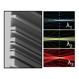 |
| This completely flat, ultrathin lens can focus different wavelengths of light at the same point, achieving instant color correction in one extremely thin, miniaturized device. Image courtesy of Federico Capasso and Francesco Aieta, Harvard SEAS |
Abstract:
Most lenses are, by definition, curved. After all, they are named for their resemblance to lentils, and a glass lens made flat is just a window with no special powers.
Perfect colors, captured with one ultra-thin lens: No need for color correction -- Harvard physicists' flat optics, using nanotechnology, get it right the first time
Cambridge, MA | Posted on February 19th, 2015But a new type of lens created at the Harvard School of Engineering and Applied Sciences (SEAS) turns conventional optics on its head.
A major leap forward from a prototype device demonstrated in 2012, it is an ultra-thin, completely flat optical component made of a glass substrate and tiny, light-concentrating silicon antennas. Light shining on it bends instantaneously, rather than gradually, while passing through. The bending effects can be designed in advance, by an algorithm, and fine-tuned to fit almost any purpose.
With this new invention described today in Science, the Harvard research team has overcome an inherent drawback of a wafer-thin lens: light at different wavelengths (i.e., colors) responds to the surface very differently. Until now, this phenomenon has prevented planar optics from being used with broadband light. Now, instead of treating all wavelengths equally, the researchers have devised a flat lens with antennas that compensate for the wavelength differences and produce a consistent effect--for example, deflecting three beams of different colors by the same angle, or focusing those colors on a single spot.
"What this now means is that complicated effects like color correction, which in a conventional optical system would require light to pass through several thick lenses in sequence, can be achieved in one extremely thin, miniaturized device," said principal investigator Federico Capasso, the Robert L. Wallace Professor of Applied Physics and Vinton Hayes Senior Research Fellow in Electrical Engineering at Harvard SEAS.
Bernard Kress, Principal Optical Architect at Google [X], who was not involved in the research, hailed the advance:
"Google [X], and especially the Google Glass group, is relying heavily on state-of-the-art optical technologies to develop products that have higher functionalities, are easier to mass produce, have a smaller footprint, and are lighter, without compromising efficiency," he said. "Last year, we challenged Professor Capasso's group to work towards a goal which was until now unreachable by flat optics. While there are many ways to design achromatic optics, there was until now no solution to implement a dispersionless flat optical element which at the same time had uniform efficiency and the same diffraction angle for three separate wavelengths. We are very happy that Professor Capasso did accept the challenge, and also were very surprised to learn that his group actually solved that challenge within one year."
The team of researchers, led by Capasso and postdoctoral fellow Francesco Aieta, has developed a design that rivals the bulky equipment currently used in photography, astronomy, and microscopy. It could also enable the creation of new miniature optical communications devices and find application in compact cameras and imaging devices.
The new lens, dubbed an "achromatic metasurface," dramatically improves on the flat lens Capasso's research group demonstrated in 2012. That prototype, the first of its kind, corrected for some of the aberrations of conventional lenses but suffered from the limitation of only focusing light of a single wavelength, and its focusing efficiency was small. The new model uses a dielectric material rather than a metal for the nanoantennas, a change which greatly improves its efficiency and, combined with a new design approach, enables operation over a broad range of wavelengths.
Most significantly, the new design enables the creation of two different flat optical devices. The first, instead of sending different colors in different directions like a conventional grating, deflects three wavelengths of light by exactly the same angle. In the second device, the three wavelengths can all be focused at the same point. A flat lens can thus create a color image--focusing for example red, green, and blue, the primary colors used in most digital displays. The team's computational simulations also suggest that a similar architecture can be used to create a lens that collimates many different wavelengths, not just three.
"This is a major step forward in establishing a planar optical technology with a small footprint which overcomes the limitations of standard flat optics, known as diffractive optics," said Capasso. "It also opens the door to new functionalities because of the enormous design space made possible by metasurfaces."
"This is an elegant and groundbreaking accomplishment," said Nader Engheta, H. Nedwill Ramsey Professor at the University of Pennsylvania, who was not involved in the research. "The planar optical structures designed and demonstrated by Professor Capasso's group have much less volume than their conventional bulky counterparts and at the same time their chromatic aberration has been suppressed. This is an important development that will undoubtedly lead to other exciting innovations in the field of flat photonics."
Harvard's Office of Technology Development has filed for a provisional patent on the new optical technology and is actively pursuing commercial opportunities.
"Our previous work on the metallic flat lens produced a great excitement in regard to the possibility of achieving high numerical aperture and spherical aberration-free focusing with a very compact design. By demonstrating achromatic lenses we have now made a major step forward towards widespread future application of flat optics that will certainly attract the interest of the industry," said lead author Francesco Aieta, now employed by Hewlett Packard, who conducted the research at Harvard SEAS.
###
Additional coauthors of the Science paper include Mikhail A. Kats and Patrice Genevet, both former members of the Capasso laboratory. Kats, who earned his Ph.D. at Harvard SEAS in 2013, is now an assistant professor at the University of Wisconsin, Madison. Genevet, formerly a postdoctoral research associate at SEAS, is now at the Singapore Institute of Manufacturing Technology.
This research was supported in part by a MURI grant from the Air Force Office of Scientific Research (FA9550-12-1-0389), with additional support from Draper Laboratory (SC001-0000000731), and the National Science Foundation (NSF, ECCS-1347251). Fabrication was performed at the Harvard Center for Nanoscale Systems, which is a member of the NSF-funded National Nanotechnology Infrastructure Network.
####
For more information, please click here
Contacts:
Caroline Perry
617-496-1351
Copyright © Harvard University
If you have a comment, please Contact us.Issuers of news releases, not 7th Wave, Inc. or Nanotechnology Now, are solely responsible for the accuracy of the content.
Bookmark:


| Related News Press |
News and information
![]() Quantum computer improves AI predictions April 17th, 2026
Quantum computer improves AI predictions April 17th, 2026
![]() Flexible sensor gains sensitivity under pressure April 17th, 2026
Flexible sensor gains sensitivity under pressure April 17th, 2026
![]() A reusable chip for particulate matter sensing April 17th, 2026
A reusable chip for particulate matter sensing April 17th, 2026
![]() Detecting vibrational quantum beating in the predissociation dynamics of SF6 using time-resolved photoelectron spectroscopy April 17th, 2026
Detecting vibrational quantum beating in the predissociation dynamics of SF6 using time-resolved photoelectron spectroscopy April 17th, 2026
Imaging
![]() Simple algorithm paired with standard imaging tool could predict failure in lithium metal batteries August 8th, 2025
Simple algorithm paired with standard imaging tool could predict failure in lithium metal batteries August 8th, 2025
Govt.-Legislation/Regulation/Funding/Policy
![]() Quantum computer improves AI predictions April 17th, 2026
Quantum computer improves AI predictions April 17th, 2026
![]() Metasurfaces smooth light to boost magnetic sensing precision January 30th, 2026
Metasurfaces smooth light to boost magnetic sensing precision January 30th, 2026
![]() New imaging approach transforms study of bacterial biofilms August 8th, 2025
New imaging approach transforms study of bacterial biofilms August 8th, 2025
Discoveries
![]() Quantum computer improves AI predictions April 17th, 2026
Quantum computer improves AI predictions April 17th, 2026
![]() Flexible sensor gains sensitivity under pressure April 17th, 2026
Flexible sensor gains sensitivity under pressure April 17th, 2026
![]() A reusable chip for particulate matter sensing April 17th, 2026
A reusable chip for particulate matter sensing April 17th, 2026
![]() Detecting vibrational quantum beating in the predissociation dynamics of SF6 using time-resolved photoelectron spectroscopy April 17th, 2026
Detecting vibrational quantum beating in the predissociation dynamics of SF6 using time-resolved photoelectron spectroscopy April 17th, 2026
Announcements
![]() A fundamentally new therapeutic approach to cystic fibrosis: Nanobody repairs cellular defect April 17th, 2026
A fundamentally new therapeutic approach to cystic fibrosis: Nanobody repairs cellular defect April 17th, 2026
![]() UC Irvine physicists discover method to reverse �quantum scrambling� : The work addresses the problem of information loss in quantum computing system April 17th, 2026
UC Irvine physicists discover method to reverse �quantum scrambling� : The work addresses the problem of information loss in quantum computing system April 17th, 2026
Interviews/Book Reviews/Essays/Reports/Podcasts/Journals/White papers/Posters
![]() A fundamentally new therapeutic approach to cystic fibrosis: Nanobody repairs cellular defect April 17th, 2026
A fundamentally new therapeutic approach to cystic fibrosis: Nanobody repairs cellular defect April 17th, 2026
![]() UC Irvine physicists discover method to reverse �quantum scrambling� : The work addresses the problem of information loss in quantum computing system April 17th, 2026
UC Irvine physicists discover method to reverse �quantum scrambling� : The work addresses the problem of information loss in quantum computing system April 17th, 2026
Tools
![]() Metasurfaces smooth light to boost magnetic sensing precision January 30th, 2026
Metasurfaces smooth light to boost magnetic sensing precision January 30th, 2026
![]() From sensors to smart systems: the rise of AI-driven photonic noses January 30th, 2026
From sensors to smart systems: the rise of AI-driven photonic noses January 30th, 2026
![]() Japan launches fully domestically produced quantum computer: Expo visitors to experience quantum computing firsthand August 8th, 2025
Japan launches fully domestically produced quantum computer: Expo visitors to experience quantum computing firsthand August 8th, 2025
Military
![]() Quantum engineers �squeeze� laser frequency combs to make more sensitive gas sensors January 17th, 2025
Quantum engineers �squeeze� laser frequency combs to make more sensitive gas sensors January 17th, 2025
![]() Chainmail-like material could be the future of armor: First 2D mechanically interlocked polymer exhibits exceptional flexibility and strength January 17th, 2025
Chainmail-like material could be the future of armor: First 2D mechanically interlocked polymer exhibits exceptional flexibility and strength January 17th, 2025
![]() Single atoms show their true color July 5th, 2024
Single atoms show their true color July 5th, 2024
![]() NRL charters Navy�s quantum inertial navigation path to reduce drift April 5th, 2024
NRL charters Navy�s quantum inertial navigation path to reduce drift April 5th, 2024
Photonics/Optics/Lasers
![]() Metasurfaces smooth light to boost magnetic sensing precision January 30th, 2026
Metasurfaces smooth light to boost magnetic sensing precision January 30th, 2026
![]() From sensors to smart systems: the rise of AI-driven photonic noses January 30th, 2026
From sensors to smart systems: the rise of AI-driven photonic noses January 30th, 2026
Research partnerships
![]() Lab to industry: InSe wafer-scale breakthrough for future electronics August 8th, 2025
Lab to industry: InSe wafer-scale breakthrough for future electronics August 8th, 2025
![]() HKU physicists uncover hidden order in the quantum world through deconfined quantum critical points April 25th, 2025
HKU physicists uncover hidden order in the quantum world through deconfined quantum critical points April 25th, 2025
|
|
||
|
|
||
| The latest news from around the world, FREE | ||
|
|
||
|
|
||
| Premium Products | ||
|
|
||
|
Only the news you want to read!
Learn More |
||
|
|
||
|
Full-service, expert consulting
Learn More |
||
|
|
||