Home > Press > New signal amplification process set to transform communications, imaging, computing: UC San Diego researchers discover a mechanism to amplify signals in optoelectronic systems that is far more efficient than standard processes
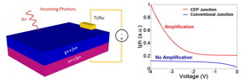 |
| This schematic illustrates the concepts involved in the cycling excitation process. CREDIT:Yuchun Zhou/UCSD |
Abstract:
Signal amplification is ubiquitous to all electronic and optoelectronic systems for communications, imaging and computing - its characteristics directly impact device performance.
New signal amplification process set to transform communications, imaging, computing: UC San Diego researchers discover a mechanism to amplify signals in optoelectronic systems that is far more efficient than standard processes
Washington, DC | Posted on January 21st, 2015A new signal amplification process discovered by a team of University of California, San Diego researchers is now poised to fuel new generations of electrical and photonic devices - transforming the fields of communications, imaging and computing. In the journal Applied Physics Letters, from AIP Publishing, the team describes their work behind this discovery.
"For many years, the semiconductor industry has relied on photodetectors for optoelectrical conversion, followed by low-noise electronic amplifiers to convert optical signals into electronic signals with amplification to enable information detection and processing," explained Yu-Hwa Lo, a professor of electrical and computer engineering at the University of California, San Diego.
It's also widely recognized that the highest sensitivity can be achieved by combining an electronic amplifier with a photodetector that uses an internal amplification mechanism to optimally balance out the thermal noise of the electronic amplifier and the shot noise, a type of noise in the photodetector that arises because of the particle nature of light.
"Following this established principle, avalanche photodetectors that use impact ionization became the devices of choice and have remained so for many decades," Lo noted. Impact ionization, however, has drawbacks such as high operation voltage - typically 30 to 200V - and rapidly increasing noise with amplification.
So the team searched for a more efficient intrinsic amplification mechanism for semiconductors to amplify the photocurrent at much lower voltage and noise than the current method.
"Thanks to insights of the complex interactions among electrons in localized and extended states and phonons (a unit of vibrational energy that arises from oscillating atoms within a crystal), we've discovered a far more efficient mechanism - the cycling excitation process (CEP) - to amplify the signal," Lo said.
Ready to delve into the technical concepts involved? The device primarily has a p/n junction (a boundary between two semiconductor materials within a single crystal of semiconductor) similar to those found in semiconductor devices. "The only unique feature is that both sides of the p/n junction contain a substantial amount of counter doping - a large number of donors exist in the p-region, with acceptors in the n-region," explained Lo. Such a structure is called a "heavily compensated p/n junction."
Counter impurities in the compensated p/n junction are responsible for the team's highly efficient signal (photocurrent) amplification process. Electrons or holes crossing the depletion region gain kinetic energy and, in turn, excite new electron-hole pairs using the compensating impurities (donors in the p-side and acceptors in the n-side) as intermediate states.
"An energetic electron, for example, can excite an electron from an occupied acceptor to the conduction band, while a phonon is absorbed subsequently to fill the acceptor with an electron from the valence band - producing a hole in the valence band to complete the generation of an electron-hole pair," said Yuchun Zhou, first author of the paper and a doctoral student in Lo's group. "This type of process occurs on both sides of the p/n junction and forms cycles of electron-hole excitation to produce high gain."
The key discovery and innovation for the amplification process is to use the compensating impurities as the intermediate steps for electron-hole pair generation. "Impurity states are localized, so the conservation of momentum that limits the efficiency for conventional impact ionization can be greatly relaxed and leads to higher signal amplification efficiency and reduced operation voltage," added Lo.
Most striking implication of the team's discovery? "Perhaps that an entirely new physical mechanism can be found in the most common device structure - a p/n junction - that has been used since the semiconductor industry's heyday," said Lo. "It appears that a small modification, such as heavy doping compensation, from a common structure can be used to take advantage of the unusual physical process that results from concerted interactions between electrons in extended and localized (impurity) states and phonons."
With further improvements, according to the team, the discovered signal amplification mechanism can be used in a wide variety of devices and semiconductors - presenting a new paradigm for the semiconductor industry.
"With an efficient gain mechanism at an operation voltage compatible with CMOS integrated circuits, it's possible to produce communication and imaging devices with superior sensitivity at a low cost," Lo pointed out. "By using other methods along with optical excitation to produce the seed carriers that initiate the cycling excitation process, we can conceive new types of transistors and circuits and extend the scope of applications beyond optical detection."
####
About American Institute of Physics
Applied Physics Letters features concise, rapid reports on significant new findings in applied physics. The journal covers new experimental and theoretical research on applications of physics phenomena related to all branches of science, engineering, and modern technology. See: apl.aip.org
For more information, please click here
Contacts:
Jason Socrates Bardi
240-535-4954
Copyright © American Institute of Physics
If you have a comment, please Contact us.Issuers of news releases, not 7th Wave, Inc. or Nanotechnology Now, are solely responsible for the accuracy of the content.
Bookmark:


| Related Links |
| Related News Press |
News and information
![]() Quantum computer improves AI predictions April 17th, 2026
Quantum computer improves AI predictions April 17th, 2026
![]() Flexible sensor gains sensitivity under pressure April 17th, 2026
Flexible sensor gains sensitivity under pressure April 17th, 2026
![]() A reusable chip for particulate matter sensing April 17th, 2026
A reusable chip for particulate matter sensing April 17th, 2026
![]() Detecting vibrational quantum beating in the predissociation dynamics of SF6 using time-resolved photoelectron spectroscopy April 17th, 2026
Detecting vibrational quantum beating in the predissociation dynamics of SF6 using time-resolved photoelectron spectroscopy April 17th, 2026
Wireless/telecommunications/RF/Antennas/Microwaves
![]() Researchers develop molecular qubits that communicate at telecom frequencies October 3rd, 2025
Researchers develop molecular qubits that communicate at telecom frequencies October 3rd, 2025
![]() HKUST researchers develop new integration technique for efficient coupling of III-V and silicon February 16th, 2024
HKUST researchers develop new integration technique for efficient coupling of III-V and silicon February 16th, 2024
Chip Technology
![]() A reusable chip for particulate matter sensing April 17th, 2026
A reusable chip for particulate matter sensing April 17th, 2026
![]() Metasurfaces smooth light to boost magnetic sensing precision January 30th, 2026
Metasurfaces smooth light to boost magnetic sensing precision January 30th, 2026
Optical computing/Photonic computing
![]() ICFO researchers overcome long-standing bottleneck in single photon detection with twisted 2D materials August 8th, 2025
ICFO researchers overcome long-standing bottleneck in single photon detection with twisted 2D materials August 8th, 2025
![]() Programmable electron-induced color router array May 14th, 2025
Programmable electron-induced color router array May 14th, 2025
Discoveries
![]() Quantum computer improves AI predictions April 17th, 2026
Quantum computer improves AI predictions April 17th, 2026
![]() Flexible sensor gains sensitivity under pressure April 17th, 2026
Flexible sensor gains sensitivity under pressure April 17th, 2026
![]() A reusable chip for particulate matter sensing April 17th, 2026
A reusable chip for particulate matter sensing April 17th, 2026
![]() Detecting vibrational quantum beating in the predissociation dynamics of SF6 using time-resolved photoelectron spectroscopy April 17th, 2026
Detecting vibrational quantum beating in the predissociation dynamics of SF6 using time-resolved photoelectron spectroscopy April 17th, 2026
Announcements
![]() A fundamentally new therapeutic approach to cystic fibrosis: Nanobody repairs cellular defect April 17th, 2026
A fundamentally new therapeutic approach to cystic fibrosis: Nanobody repairs cellular defect April 17th, 2026
![]() UC Irvine physicists discover method to reverse �quantum scrambling� : The work addresses the problem of information loss in quantum computing system April 17th, 2026
UC Irvine physicists discover method to reverse �quantum scrambling� : The work addresses the problem of information loss in quantum computing system April 17th, 2026
Interviews/Book Reviews/Essays/Reports/Podcasts/Journals/White papers/Posters
![]() A fundamentally new therapeutic approach to cystic fibrosis: Nanobody repairs cellular defect April 17th, 2026
A fundamentally new therapeutic approach to cystic fibrosis: Nanobody repairs cellular defect April 17th, 2026
![]() UC Irvine physicists discover method to reverse �quantum scrambling� : The work addresses the problem of information loss in quantum computing system April 17th, 2026
UC Irvine physicists discover method to reverse �quantum scrambling� : The work addresses the problem of information loss in quantum computing system April 17th, 2026
Photonics/Optics/Lasers
![]() Metasurfaces smooth light to boost magnetic sensing precision January 30th, 2026
Metasurfaces smooth light to boost magnetic sensing precision January 30th, 2026
![]() From sensors to smart systems: the rise of AI-driven photonic noses January 30th, 2026
From sensors to smart systems: the rise of AI-driven photonic noses January 30th, 2026
|
|
||
|
|
||
| The latest news from around the world, FREE | ||
|
|
||
|
|
||
| Premium Products | ||
|
|
||
|
Only the news you want to read!
Learn More |
||
|
|
||
|
Full-service, expert consulting
Learn More |
||
|
|
||