Home > Press > Solving an organic semiconductor mystery: Berkeley Lab researchers uncover hidden structures in domain interfaces that hamper performance
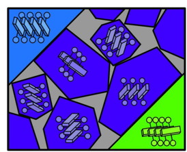 |
| Sketch of organic semiconductor thin film shows that the interfacial region between larger domains (blue and green) consists of randomly oriented small, nano-crystalline domains (purple).
CREDIT: Image courtesy of Naomi Ginsberg, Berkeley Lab |
Abstract:
Organic semiconductors are prized for light emitting diodes (LEDs), field effect transistors (FETs) and photovoltaic cells. As they can be printed from solution, they provide a highly scalable, cost-effective alternative to silicon-based devices. Uneven performances, however, have been a persistent problem. Scientists have known that the performance issues originate in the domain interfaces within organic semiconductor thin films, but have not known the cause. This mystery now appears to have been solved.
Solving an organic semiconductor mystery: Berkeley Lab researchers uncover hidden structures in domain interfaces that hamper performance
Berkeley, CA | Posted on January 16th, 2015Naomi Ginsberg, a faculty chemist with the U.S. Department of Energy (DOE)'s Lawrence Berkeley National Laboratory and the University of California (UC) Berkeley, led a team that used a unique form of microscopy to study the domain interfaces within an especially high-performing solution-processed organic semiconductor called TIPS-pentacene. She and her team discovered a cluttered jumble of randomly oriented nanocrystallites that become kinetically trapped in the interfaces during solution casting. Like debris on a highway, these nanocrystallites impede the flow of charge-carriers.
"If the interfaces were neat and clean, they wouldn't have such a large impact on performance, but the presence of the nanocrystallites reduces charge-carrier mobility," Ginsberg says. "Our nanocrystallite model for the interface, which is consistent with observations, provides critical information that can be used to correlate solution-processing methods to optimal device performances."
Ginsberg, who holds appointments with Berkeley Lab's Physical Biosciences Division and its Materials Sciences Division, as well as UC Berkeley's departments of chemistry and physics, is the corresponding author of a paper describing this research in Nature Communications. The paper is titled "Exciton dynamics reveals aggregates with intermolecular order at hidden interfaces in solution-cast organic semiconducting films." Co-authors are Cathy Wong, Benjamin Cotts and Hao Wu.
Organic semiconductors are based on the ability of carbon to form larger molecules, such as benzene and pentacene, featuring electrical conductivity that falls somewhere between insulators and metals. Through solution-processing, organic materials can usually be fashioned into crystalline films without the expensive high-temperature annealing process required for silicon and other inorganic semiconductors. However, even though it has long been clear that the crystalline domain interfaces within semiconductor organic thin films are critical to their performance in devices, detailed information on the morphology of these interfaces has been missing until now.
"Interface domains in organic semiconductor thin films are smaller than the diffraction limit, hidden from surface probe techniques such as atomic force microscopy, and their nanoscale heterogeneity is not typically resolved using X-ray methods," Ginsberg says. "Furthermore, the crystalline TIPS-pentacene we studied has virtually zero emission, which means it can't be studied with photoluminescence microscopy."
Ginsberg and her group overcame the challenges by using transient absorption (TA) microscopy, a technique in which femtosecond laser pulses excite transient energy states and detectors measure the changes in the absorption spectra. The Berkeley researchers carried out TA microscopy on an optical microscope they constructed themselves that enabled them to generate focal volumes that are a thousand times smaller than is typical for conventional TA microscopes. They also deployed multiple different light polarizations that allowed them to isolate interface signals not seen in either of the adjacent domains.
"Instrumentation, including very good detectors, the painstaking collection of data to ensure good signal-to-noise ratios, and the way we crafted the experiment and analysis were all critical to our success," Ginsberg says. "Our spatial resolution and light polarization sensitivity were also essential to be able to unequivocally see a signature of the interface that was not swamped by the bulk, which contributes much more to the raw signal by volume."
The methology developed by Ginsberg and her team to uncover structural motifs at hidden interfaces in organic semiconductor thin films should add a predictive factor to scalable and affordable solution-processing of these materials. This predictive capability should help minimize discontinuities and maximize charge-carrier mobility. Currently, researchers use what is essentially a trial-and-error approach, in which different solution casting conditions are tested to see how well the resulting devices perform.
"Our methodology provides an important intermediary in the feedback loop of device optimization by characterizing the microscopic details of the films that go into the devices, and by inferring how the solution casting could have created the structures at the interfaces," Ginsberg says. "As a result, we can suggest how to alter the delicate balance of solution casting parameters to make more functional films."
###
This research was primarily funded by the Defense Advanced Research Projects Agency.
####
About DOE/Lawrence Berkeley National Laboratory
Lawrence Berkeley National Laboratory addresses the world's most urgent scientific challenges by advancing sustainable energy, protecting human health, creating new materials, and revealing the origin and fate of the universe. Founded in 1931, Berkeley Lab's scientific expertise has been recognized with 13 Nobel prizes. The University of California manages Berkeley Lab for the U.S. Department of Energy's Office of Science. For more, visit www.lbl.gov.
For more information, please click here
Contacts:
Lynn Yarris
510-486-5375
Copyright © DOE/Lawrence Berkeley National Laboratory
If you have a comment, please Contact us.Issuers of news releases, not 7th Wave, Inc. or Nanotechnology Now, are solely responsible for the accuracy of the content.
Bookmark:


| Related News Press |
News and information
![]() Quantum computer improves AI predictions April 17th, 2026
Quantum computer improves AI predictions April 17th, 2026
![]() Flexible sensor gains sensitivity under pressure April 17th, 2026
Flexible sensor gains sensitivity under pressure April 17th, 2026
![]() A reusable chip for particulate matter sensing April 17th, 2026
A reusable chip for particulate matter sensing April 17th, 2026
![]() Detecting vibrational quantum beating in the predissociation dynamics of SF6 using time-resolved photoelectron spectroscopy April 17th, 2026
Detecting vibrational quantum beating in the predissociation dynamics of SF6 using time-resolved photoelectron spectroscopy April 17th, 2026
Imaging
![]() Simple algorithm paired with standard imaging tool could predict failure in lithium metal batteries August 8th, 2025
Simple algorithm paired with standard imaging tool could predict failure in lithium metal batteries August 8th, 2025
![]() First real-time observation of two-dimensional melting process: Researchers at Mainz University unveil new insights into magnetic vortex structures August 8th, 2025
First real-time observation of two-dimensional melting process: Researchers at Mainz University unveil new insights into magnetic vortex structures August 8th, 2025
![]() New imaging approach transforms study of bacterial biofilms August 8th, 2025
New imaging approach transforms study of bacterial biofilms August 8th, 2025
Physics
![]() UC Irvine physicists discover method to reverse �quantum scrambling� : The work addresses the problem of information loss in quantum computing system April 17th, 2026
UC Irvine physicists discover method to reverse �quantum scrambling� : The work addresses the problem of information loss in quantum computing system April 17th, 2026
Thin films
![]() Tiny nanosheets, big leap: A new sensor detects ethanol at ultra-low levels January 30th, 2026
Tiny nanosheets, big leap: A new sensor detects ethanol at ultra-low levels January 30th, 2026
Laboratories
![]() Researchers develop molecular qubits that communicate at telecom frequencies October 3rd, 2025
Researchers develop molecular qubits that communicate at telecom frequencies October 3rd, 2025
Govt.-Legislation/Regulation/Funding/Policy
![]() Quantum computer improves AI predictions April 17th, 2026
Quantum computer improves AI predictions April 17th, 2026
![]() Metasurfaces smooth light to boost magnetic sensing precision January 30th, 2026
Metasurfaces smooth light to boost magnetic sensing precision January 30th, 2026
![]() New imaging approach transforms study of bacterial biofilms August 8th, 2025
New imaging approach transforms study of bacterial biofilms August 8th, 2025
Chip Technology
![]() A reusable chip for particulate matter sensing April 17th, 2026
A reusable chip for particulate matter sensing April 17th, 2026
![]() Metasurfaces smooth light to boost magnetic sensing precision January 30th, 2026
Metasurfaces smooth light to boost magnetic sensing precision January 30th, 2026
Discoveries
![]() Quantum computer improves AI predictions April 17th, 2026
Quantum computer improves AI predictions April 17th, 2026
![]() Flexible sensor gains sensitivity under pressure April 17th, 2026
Flexible sensor gains sensitivity under pressure April 17th, 2026
![]() A reusable chip for particulate matter sensing April 17th, 2026
A reusable chip for particulate matter sensing April 17th, 2026
![]() Detecting vibrational quantum beating in the predissociation dynamics of SF6 using time-resolved photoelectron spectroscopy April 17th, 2026
Detecting vibrational quantum beating in the predissociation dynamics of SF6 using time-resolved photoelectron spectroscopy April 17th, 2026
Announcements
![]() A fundamentally new therapeutic approach to cystic fibrosis: Nanobody repairs cellular defect April 17th, 2026
A fundamentally new therapeutic approach to cystic fibrosis: Nanobody repairs cellular defect April 17th, 2026
![]() UC Irvine physicists discover method to reverse �quantum scrambling� : The work addresses the problem of information loss in quantum computing system April 17th, 2026
UC Irvine physicists discover method to reverse �quantum scrambling� : The work addresses the problem of information loss in quantum computing system April 17th, 2026
Interviews/Book Reviews/Essays/Reports/Podcasts/Journals/White papers/Posters
![]() A fundamentally new therapeutic approach to cystic fibrosis: Nanobody repairs cellular defect April 17th, 2026
A fundamentally new therapeutic approach to cystic fibrosis: Nanobody repairs cellular defect April 17th, 2026
![]() UC Irvine physicists discover method to reverse �quantum scrambling� : The work addresses the problem of information loss in quantum computing system April 17th, 2026
UC Irvine physicists discover method to reverse �quantum scrambling� : The work addresses the problem of information loss in quantum computing system April 17th, 2026
Tools
![]() Metasurfaces smooth light to boost magnetic sensing precision January 30th, 2026
Metasurfaces smooth light to boost magnetic sensing precision January 30th, 2026
![]() From sensors to smart systems: the rise of AI-driven photonic noses January 30th, 2026
From sensors to smart systems: the rise of AI-driven photonic noses January 30th, 2026
![]() Japan launches fully domestically produced quantum computer: Expo visitors to experience quantum computing firsthand August 8th, 2025
Japan launches fully domestically produced quantum computer: Expo visitors to experience quantum computing firsthand August 8th, 2025
Military
![]() Quantum engineers �squeeze� laser frequency combs to make more sensitive gas sensors January 17th, 2025
Quantum engineers �squeeze� laser frequency combs to make more sensitive gas sensors January 17th, 2025
![]() Chainmail-like material could be the future of armor: First 2D mechanically interlocked polymer exhibits exceptional flexibility and strength January 17th, 2025
Chainmail-like material could be the future of armor: First 2D mechanically interlocked polymer exhibits exceptional flexibility and strength January 17th, 2025
![]() Single atoms show their true color July 5th, 2024
Single atoms show their true color July 5th, 2024
![]() NRL charters Navy�s quantum inertial navigation path to reduce drift April 5th, 2024
NRL charters Navy�s quantum inertial navigation path to reduce drift April 5th, 2024
|
|
||
|
|
||
| The latest news from around the world, FREE | ||
|
|
||
|
|
||
| Premium Products | ||
|
|
||
|
Only the news you want to read!
Learn More |
||
|
|
||
|
Full-service, expert consulting
Learn More |
||
|
|
||