Home > Press > Powerful new technique simultaneously determines nanomaterials' chemical makeup, topography
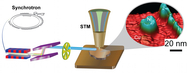 |
| The synchrotron X-ray scanning tunneling microscopy concept allowed Argonne National Laboratory and Ohio University researchers to achieve a recording-breaking resolution of a nanoscale material. They combined of a synchrotron X-ray as a probe and a nanofabricated smart tip as a detector to fingerprint individual nickel clusters on a copper surface at a two-nanometer resolution and at the ultimate single-atomic height sensitivity. And by varying the photon energy, researchers successfully measured photoionization cross sections of a single nickel nanocluster � opening the door to new opportunities for chemical imaging of nanoscale materials. |
Abstract:
A team of researchers from the U.S. Department of Energy's Argonne National Laboratory and Ohio University have devised a powerful technique that simultaneously resolves the chemical characterization and topography of nanoscale materials down to the height of a single atom.
Powerful new technique simultaneously determines nanomaterials' chemical makeup, topography
Argonne, IL | Posted on December 2nd, 2014The technique combines synchrotron X-rays (SX) and scanning tunneling microscopy (STM). In experiments, the researchers used SX as a probe and a nanofabricated smart tip of a STM as a detector.
Using this technique, researchers detected the chemical fingerprint of individual nickel clusters on a copper surface at a two-nanometer (nm) lateral resolution, and at the ultimate single atom height sensitivity. By varying the photon energy, the researchers used the difference in photoabsorption cross sections for nickel and the copper substrate to chemically image a single-nickel nanocluster - thus opening the door to new opportunities for chemical imaging of nanoscale materials. Until now, a spatial limit of about only 10-nm was attainable, and the researchers would simultaneously sample a large sample area. The researchers have improved the spatial resolution to 2 nm.
"Imaging with direct chemical sensitivity has been a long-standing goal since scanning tunneling microscopes were developed during the 1980s," said Volker Rose, a physicist in the X-ray Science Division. "It was very exciting when we obtained elemental contrast of a material at just one atomic layer height".
"This is a marriage between two of the most powerful instruments of materials science," said Saw-Wai Hla, electronic and magnetic materials and devices group leader in Argonne's Nanoscience & Technology Division. "We now have an instrument that can perform the functions of STM and X-rays in a single setting, and therefore it has a great potential to revolutionize the materials characterization."
To conduct the experiment, researchers used the Center for Nanoscale Materials' (CNM) beamline 26-ID at the Advanced Photon Source (APS), which is equipped with two collinear undulator devices that serve as the X-ray source and a double-crystal monochromater that selects the photon energy. The X-rays were passed through a beam chopper to quickly turn the beam on and off and then illuminate the tip/sample junction in the SX-STM. This enabled the very sensitive lock-in detection of the X-ray induced currents.
The experiment was conducted at room temperature, which is well suited for the needs of most physical, chemical, biological and nanomaterial applications. The team anticipates that even higher spatial resolution may become possible with a new instrument currently under development.
"The next step will be to extend the new technique to low temperatures," notes Rose. "Our measurements indicate that atomic resolution may be achievable at 5 K (about negative 450 F)."
This research was funded by the DOE Office of Science Early Career Research Program. The APS and CNM are DOE Office of Science User Facilities located at Argonne.
Nozomi Shirato, Marvin Cummings and Benjamin Stripe, postdoctoral appointees at Argonne, and Heath Kersell and Yang Li, graduate students in physics at Ohio University, helped to conduct the experiments. Saw-Wai Hla and Volker Rose, of Argonne, designed the experiment and Daniel Rosenmann, of Argonne, made the smart tip. Curt Preissner, of Argonne's APS Engineering Support Division, provided engineering support, and Jon Hiller, formerly of CNM's Electron Microscopy Center group, helped to make the smart tip.
####
About Argonne National Laboratory
Argonne National Laboratory seeks solutions to pressing national problems in science and technology. The nation's first national laboratory, Argonne conducts leading-edge basic and applied scientific research in virtually every scientific discipline. Argonne researchers work closely with researchers from hundreds of companies, universities, and federal, state and municipal agencies to help them solve their specific problems, advance America's scientific leadership and prepare the nation for a better future. With employees from more than 60 nations. Argonne is supported by the Office of Science of the U.S. Department of Energy. The Office of Science is the single largest supporter of basic research in the physical sciences in the United States, and is working to address some of the most pressing challenges of our time. For more information, please visit science.energy.gov.�
For more information, please click here
Contacts:
Tona Kunz
630-252-5560
Copyright © Argonne National Laboratory
If you have a comment, please Contact us.Issuers of news releases, not 7th Wave, Inc. or Nanotechnology Now, are solely responsible for the accuracy of the content.
Bookmark:


| Related Links |
![]() To learn more about the project, visit the SXSPM website:
To learn more about the project, visit the SXSPM website:
| Related News Press |
News and information
![]() Quantum computer improves AI predictions April 17th, 2026
Quantum computer improves AI predictions April 17th, 2026
![]() Flexible sensor gains sensitivity under pressure April 17th, 2026
Flexible sensor gains sensitivity under pressure April 17th, 2026
![]() A reusable chip for particulate matter sensing April 17th, 2026
A reusable chip for particulate matter sensing April 17th, 2026
![]() Detecting vibrational quantum beating in the predissociation dynamics of SF6 using time-resolved photoelectron spectroscopy April 17th, 2026
Detecting vibrational quantum beating in the predissociation dynamics of SF6 using time-resolved photoelectron spectroscopy April 17th, 2026
Imaging
![]() Simple algorithm paired with standard imaging tool could predict failure in lithium metal batteries August 8th, 2025
Simple algorithm paired with standard imaging tool could predict failure in lithium metal batteries August 8th, 2025
![]() First real-time observation of two-dimensional melting process: Researchers at Mainz University unveil new insights into magnetic vortex structures August 8th, 2025
First real-time observation of two-dimensional melting process: Researchers at Mainz University unveil new insights into magnetic vortex structures August 8th, 2025
Chemistry
![]() Projecting light to dispense liquids: A new route to ultra-precise microdroplets January 30th, 2026
Projecting light to dispense liquids: A new route to ultra-precise microdroplets January 30th, 2026
![]() From sensors to smart systems: the rise of AI-driven photonic noses January 30th, 2026
From sensors to smart systems: the rise of AI-driven photonic noses January 30th, 2026
![]() "Nanoreactor" cage uses visible light for catalytic and ultra-selective cross-cycloadditions October 3rd, 2025
"Nanoreactor" cage uses visible light for catalytic and ultra-selective cross-cycloadditions October 3rd, 2025
Laboratories
![]() Researchers develop molecular qubits that communicate at telecom frequencies October 3rd, 2025
Researchers develop molecular qubits that communicate at telecom frequencies October 3rd, 2025
Govt.-Legislation/Regulation/Funding/Policy
![]() Quantum computer improves AI predictions April 17th, 2026
Quantum computer improves AI predictions April 17th, 2026
![]() Metasurfaces smooth light to boost magnetic sensing precision January 30th, 2026
Metasurfaces smooth light to boost magnetic sensing precision January 30th, 2026
![]() New imaging approach transforms study of bacterial biofilms August 8th, 2025
New imaging approach transforms study of bacterial biofilms August 8th, 2025
Discoveries
![]() Quantum computer improves AI predictions April 17th, 2026
Quantum computer improves AI predictions April 17th, 2026
![]() Flexible sensor gains sensitivity under pressure April 17th, 2026
Flexible sensor gains sensitivity under pressure April 17th, 2026
![]() A reusable chip for particulate matter sensing April 17th, 2026
A reusable chip for particulate matter sensing April 17th, 2026
![]() Detecting vibrational quantum beating in the predissociation dynamics of SF6 using time-resolved photoelectron spectroscopy April 17th, 2026
Detecting vibrational quantum beating in the predissociation dynamics of SF6 using time-resolved photoelectron spectroscopy April 17th, 2026
Materials/Metamaterials/Magnetoresistance
![]() First real-time observation of two-dimensional melting process: Researchers at Mainz University unveil new insights into magnetic vortex structures August 8th, 2025
First real-time observation of two-dimensional melting process: Researchers at Mainz University unveil new insights into magnetic vortex structures August 8th, 2025
![]() Researchers unveil a groundbreaking clay-based solution to capture carbon dioxide and combat climate change June 6th, 2025
Researchers unveil a groundbreaking clay-based solution to capture carbon dioxide and combat climate change June 6th, 2025
![]() A 1960s idea inspires NBI researchers to study hitherto inaccessible quantum states June 6th, 2025
A 1960s idea inspires NBI researchers to study hitherto inaccessible quantum states June 6th, 2025
![]() Institute for Nanoscience hosts annual proposal planning meeting May 16th, 2025
Institute for Nanoscience hosts annual proposal planning meeting May 16th, 2025
Announcements
![]() A fundamentally new therapeutic approach to cystic fibrosis: Nanobody repairs cellular defect April 17th, 2026
A fundamentally new therapeutic approach to cystic fibrosis: Nanobody repairs cellular defect April 17th, 2026
![]() UC Irvine physicists discover method to reverse �quantum scrambling� : The work addresses the problem of information loss in quantum computing system April 17th, 2026
UC Irvine physicists discover method to reverse �quantum scrambling� : The work addresses the problem of information loss in quantum computing system April 17th, 2026
Interviews/Book Reviews/Essays/Reports/Podcasts/Journals/White papers/Posters
![]() A fundamentally new therapeutic approach to cystic fibrosis: Nanobody repairs cellular defect April 17th, 2026
A fundamentally new therapeutic approach to cystic fibrosis: Nanobody repairs cellular defect April 17th, 2026
![]() UC Irvine physicists discover method to reverse �quantum scrambling� : The work addresses the problem of information loss in quantum computing system April 17th, 2026
UC Irvine physicists discover method to reverse �quantum scrambling� : The work addresses the problem of information loss in quantum computing system April 17th, 2026
Tools
![]() Metasurfaces smooth light to boost magnetic sensing precision January 30th, 2026
Metasurfaces smooth light to boost magnetic sensing precision January 30th, 2026
![]() From sensors to smart systems: the rise of AI-driven photonic noses January 30th, 2026
From sensors to smart systems: the rise of AI-driven photonic noses January 30th, 2026
![]() Japan launches fully domestically produced quantum computer: Expo visitors to experience quantum computing firsthand August 8th, 2025
Japan launches fully domestically produced quantum computer: Expo visitors to experience quantum computing firsthand August 8th, 2025
|
|
||
|
|
||
| The latest news from around the world, FREE | ||
|
|
||
|
|
||
| Premium Products | ||
|
|
||
|
Only the news you want to read!
Learn More |
||
|
|
||
|
Full-service, expert consulting
Learn More |
||
|
|
||