Home > Press > FEI Releases New Electronics Failure Analysis Applications for Helios NanoLab DualBeam Portfolio: Dx gas chemistry enables rapid delayering of ICs, while AutoLX advanced automation simplifies sample preparation for transmission electron microscopy
 |
Abstract:
FEI (NASDAQ: FEIC) announced today the release of two new application packages for its third-generation Helios NanoLab™ DualBeam™ systems, including the latest addition to the family, the plasma-sourced Helios PFIB. The new application solutions address needs in integrated device (IC) manufacturing and failure analysis for fast plan-view delayering, and rapid, automated preparation of ultrathin samples for imaging and analysis in a transmission electron microscope (TEM). The application packages are designed to work with various configurations of the Helios platform, including liquid metal (Ga) and plasma (Xe) ion sources.
FEI Releases New Electronics Failure Analysis Applications for Helios NanoLab DualBeam Portfolio: Dx gas chemistry enables rapid delayering of ICs, while AutoLX advanced automation simplifies sample preparation for transmission electron microscopy
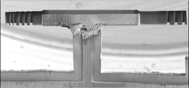
Hillsboro, OR | Posted on November 3rd, 2014"Delayering of IC devices is an important tool for semiconductor failure analysis, reverse engineering and circuit edit activities," said Rob Krueger, vice president and general manager of Electronics for FEI. "The new Dx beam chemistry delivers excellent planarity during delayering of mixed field regions, especially for technology nodes of 28nm and below where traditional methods are no longer viable. We have seen high-quality results using both Ga and Xe focused ion beams (FIBs) for front-side and back-side delayering. An additional benefit of switching to Dx for delayering is that the sidewalls of the milled trench are no longer conductive, so we can maintain device functionality if needed."
Paul Kirby, FEI's senior product marketing manager for Electronics, added, "TEM analysis is becoming nearly indispensable for process control and failure analysis at advanced nodes where device features are too small to be seen by more conventional SEM-based methods. Automated preparation of ultrathin samples that are only a few tens of nanometers thick, which is required for TEM, has contributed to greatly increased productivity and reliability of TEM analysis. The new AutoLXTM package, based on FEI's iFast Automation software, fully automates the in-situ lift out process, which locates and extracts a site-specific thick section containing the targeted feature and mounts it on a grid ready to be thinned to its final dimensions. For labs already using iFast recipes to create these thick samples, the addition of the AutoLX package opens up the door to increased productivity and more efficient use of valuable human resources."
The DualBeam's ability to visualize and manipulate structures at the nanometer scale has led to its wide-spread adoption by semiconductor manufacturers in a variety of applications, including process development and control, failure analysis, and circuit edit. The Helios NanoLab DualBeam continues FEI's well-established leadership in DualBeam instrumentation, building on a long history of performance and innovation from the first commercial DualBeam, which FEI launched more than 20 years ago.
Please visit www.fei.com/electronics for more information. Or visit FEI at the International Symposium for Testing and Failure Analysis (ISTFA), November 9-13, 2014 in Houston, Texas.
####
About FEI Company
FEI Company (Nasdaq: FEIC) designs, manufactures and supports a broad range of high-performance microscopy workflow solutions that provide images and answers at the micro-, nano- and picometer scales. Its innovation and leadership enable customers in industry and science to increase productivity and make breakthrough discoveries. Headquartered in Hillsboro, Ore., USA, FEI has over 2,600 employees and sales and service operations in more than 50 countries around the world. More information can be found at: www.fei.com.
FEI Safe Harbor Statement
This news release contains forward-looking statements that include statements regarding the performance capabilities and benefits of the Helios NanoLab DualBeam, Helios PFIB, Dx Chemistry and AutoXL package. Factors that could affect these forward-looking statements include but are not limited to our ability to manufacture, ship, deliver and install the tools or software as expected; failure of the product or technology to perform as expected; unexpected technology problems and challenges; changes to the technology; the inability of FEI, its suppliers or project partners to make the technological advances required for the technology to achieve anticipated results; and the inability of the customer to deploy the tools or develop and deploy the expected new applications. Please also refer to our Form 10-K, Forms 10-Q, Forms 8-K and other filings with the U.S. Securities and Exchange Commission for additional information on these factors and other factors that could cause actual results to differ materially from the forward-looking statements. FEI assumes no duty to update forward-looking statements.
For more information, please click here
Contacts:
Sandy Fewkes (media contact)
MindWrite Communications, Inc.
+1 408 224 4024
FEI Company
Jason Willey (investors and analysts)
Investor Relations Director
+1 503 726 2533
Copyright © FEI Company
If you have a comment, please Contact us.Issuers of news releases, not 7th Wave, Inc. or Nanotechnology Now, are solely responsible for the accuracy of the content.
Bookmark:


| Related News Press |
News and information
![]() Quantum computer improves AI predictions April 17th, 2026
Quantum computer improves AI predictions April 17th, 2026
![]() Flexible sensor gains sensitivity under pressure April 17th, 2026
Flexible sensor gains sensitivity under pressure April 17th, 2026
![]() A reusable chip for particulate matter sensing April 17th, 2026
A reusable chip for particulate matter sensing April 17th, 2026
![]() Detecting vibrational quantum beating in the predissociation dynamics of SF6 using time-resolved photoelectron spectroscopy April 17th, 2026
Detecting vibrational quantum beating in the predissociation dynamics of SF6 using time-resolved photoelectron spectroscopy April 17th, 2026
Imaging
![]() Simple algorithm paired with standard imaging tool could predict failure in lithium metal batteries August 8th, 2025
Simple algorithm paired with standard imaging tool could predict failure in lithium metal batteries August 8th, 2025
Software
![]() Visualizing nanoscale structures in real time: Open-source software enables researchers to see materials in 3D while they're still on the electron microscope August 19th, 2022
Visualizing nanoscale structures in real time: Open-source software enables researchers to see materials in 3D while they're still on the electron microscope August 19th, 2022
![]() Luisier wins SNSF Advanced Grant to develop simulation tools for nanoscale devices July 8th, 2022
Luisier wins SNSF Advanced Grant to develop simulation tools for nanoscale devices July 8th, 2022
![]() Oxford Instruments’ Atomfab® system is production-qualified at a market-leading GaN power electronics device manufacturer December 17th, 2021
Oxford Instruments’ Atomfab® system is production-qualified at a market-leading GaN power electronics device manufacturer December 17th, 2021
Chip Technology
![]() A reusable chip for particulate matter sensing April 17th, 2026
A reusable chip for particulate matter sensing April 17th, 2026
![]() Metasurfaces smooth light to boost magnetic sensing precision January 30th, 2026
Metasurfaces smooth light to boost magnetic sensing precision January 30th, 2026
Announcements
![]() A fundamentally new therapeutic approach to cystic fibrosis: Nanobody repairs cellular defect April 17th, 2026
A fundamentally new therapeutic approach to cystic fibrosis: Nanobody repairs cellular defect April 17th, 2026
![]() UC Irvine physicists discover method to reverse ‘quantum scrambling’ : The work addresses the problem of information loss in quantum computing system April 17th, 2026
UC Irvine physicists discover method to reverse ‘quantum scrambling’ : The work addresses the problem of information loss in quantum computing system April 17th, 2026
Tools
![]() Metasurfaces smooth light to boost magnetic sensing precision January 30th, 2026
Metasurfaces smooth light to boost magnetic sensing precision January 30th, 2026
![]() From sensors to smart systems: the rise of AI-driven photonic noses January 30th, 2026
From sensors to smart systems: the rise of AI-driven photonic noses January 30th, 2026
![]() Japan launches fully domestically produced quantum computer: Expo visitors to experience quantum computing firsthand August 8th, 2025
Japan launches fully domestically produced quantum computer: Expo visitors to experience quantum computing firsthand August 8th, 2025
Events/Classes
![]() Institute for Nanoscience hosts annual proposal planning meeting May 16th, 2025
Institute for Nanoscience hosts annual proposal planning meeting May 16th, 2025
![]() A New Blue: Mysterious origin of the ribbontail ray’s electric blue spots revealed July 5th, 2024
A New Blue: Mysterious origin of the ribbontail ray’s electric blue spots revealed July 5th, 2024
![]() Researchers demonstrate co-propagation of quantum and classical signals: Study shows that quantum encryption can be implemented in existing fiber networks January 20th, 2023
Researchers demonstrate co-propagation of quantum and classical signals: Study shows that quantum encryption can be implemented in existing fiber networks January 20th, 2023
|
|
||
|
|
||
| The latest news from around the world, FREE | ||
|
|
||
|
|
||
| Premium Products | ||
|
|
||
|
Only the news you want to read!
Learn More |
||
|
|
||
|
Full-service, expert consulting
Learn More |
||
|
|
||