Home > Press > NIST researchers enabled by AFM-IR to publish first nanoscale IR spectra of individual plasmonic nanostructures
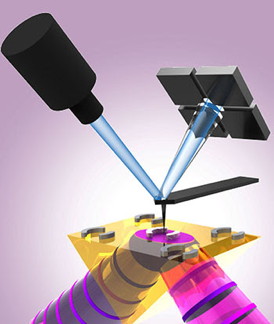 |
| Schematic showing the photothermal induced resonance (PTIR) technique: this combines the lateral resolution of atomic force microscopy (AFM) with the chemical specificity of IR spectroscopy. A wavelength-tunable, pulsed IR laser (purple) illuminates a sample consisting of plasmonic gold resonators from the below. The resulting thermal expansion of the sample is detected locally by the AFM cantilever tip, which is monitored by reflecting a laser (blue) off the back of the cantilever. Image reproduced courtesy of NIST |
Abstract:
Anasys Instruments reports on the new AFM-IR results from the Energy Research Group at NIST just published in the journal for Advanced Optical Materials. The paper is entitled "Nanoscale imaging and spectroscopy of plasmonic modes with the PTIR technique." 1
NIST researchers enabled by AFM-IR to publish first nanoscale IR spectra of individual plasmonic nanostructures
Santa Barbara, CA | Posted on October 10th, 2014Researchers from the NIST Center for Nanoscale Science and Technology (CNST) and the University of Maryland have used photothermal induced resonance (PTIR) to characterize individual plasmonic nanomaterials in order to obtain absorption maps and the first examples of absorption spectra with nanometer-scale resolution. Nanostructuring of plasmonic materials enables engineering of their resonant optical response and creates new opportunities for applications that benefit from enhanced light-matter interactions, including sensing, photovoltaics, photocatalysis, and therapeutics.
Project Leader, Andrea Centrone and his co-workers in the Energy Research Group at NIST used a technique called photothermally induced resonance (PTIR) where an AFM tip is used as an IR absorbance detector thus enabling nanoscale IR spectroscopy. Since the PTIR signal is not affected by scattering, PTIR spectra are free of Fano spectral distortions typically observed in the far-field.
Commenting on the work, Centrone says "we showed that PTIR characterization is not just applicable to organics, insulators and semiconductors, as demonstrated previously, but that metals are also amenable to it. This is an important step forward for applying the PTIR technique to a wider variety of functional devices."
PTIR is at the core of the nanoIR platform developed and supplied by Anasys Instruments for this work. Now in its second generation, the nanoIR2 combines key elements of both nanoscale IR spectroscopy and atomic force microscopy (AFM) to enable IR spectroscopy and imaging on the nanoscale. In addition to revealing chemical composition, the nanoIR2 system provides high-resolution characterization of local topographic, mechanical, and thermal properties. Potential application areas span the realms of polymer science, materials science, and life science, including detailed studies of structure property correlations.
Reference:
1) Nanoscale imaging and spectroscopy of plasmonic modes with the PTIR technique,
A. M. Katzenmeyer, J. Chae, R. Kasica, G. Holland, B. Lahiri, and A. Centrone, Advanced Optical Materials 2, 718-722 (2014).
####
About Anasys Instruments
Anasys Instruments designs breakthrough, award-winning products that deliver nanoscale probe based analytical techniques while providing high quality AFM imaging. We pioneered nanoscale IR spectroscopy, nanoscale thermal analysis and wideband nanoscale dynamic mechanical spectroscopy.
For more information, please click here
Contacts:
Anasys contact:
Roshan Shetty
Anasys Instruments Corporation
325 Chapala Street
Santa Barbara
CA 93101 USA
Tel: +1 (805) 730-3310
http://www.anasysinstruments.com/
Media contact:
Jezz Leckenby
Talking Science Limited
39 de Bohun Court
Saffron Walden
Essex CB10 2BA, UK
Tel +44 (0) 1799 521881
Mob +44 (0) 7843 012997
http://www.talking-science.com/
Copyright © Anasys Instruments
If you have a comment, please Contact us.Issuers of news releases, not 7th Wave, Inc. or Nanotechnology Now, are solely responsible for the accuracy of the content.
Bookmark:


| Related News Press |
News and information
![]() Quantum computer improves AI predictions April 17th, 2026
Quantum computer improves AI predictions April 17th, 2026
![]() Flexible sensor gains sensitivity under pressure April 17th, 2026
Flexible sensor gains sensitivity under pressure April 17th, 2026
![]() A reusable chip for particulate matter sensing April 17th, 2026
A reusable chip for particulate matter sensing April 17th, 2026
![]() Detecting vibrational quantum beating in the predissociation dynamics of SF6 using time-resolved photoelectron spectroscopy April 17th, 2026
Detecting vibrational quantum beating in the predissociation dynamics of SF6 using time-resolved photoelectron spectroscopy April 17th, 2026
Imaging
![]() Simple algorithm paired with standard imaging tool could predict failure in lithium metal batteries August 8th, 2025
Simple algorithm paired with standard imaging tool could predict failure in lithium metal batteries August 8th, 2025
![]() First real-time observation of two-dimensional melting process: Researchers at Mainz University unveil new insights into magnetic vortex structures August 8th, 2025
First real-time observation of two-dimensional melting process: Researchers at Mainz University unveil new insights into magnetic vortex structures August 8th, 2025
![]() New imaging approach transforms study of bacterial biofilms August 8th, 2025
New imaging approach transforms study of bacterial biofilms August 8th, 2025
Laboratories
![]() Researchers develop molecular qubits that communicate at telecom frequencies October 3rd, 2025
Researchers develop molecular qubits that communicate at telecom frequencies October 3rd, 2025
Govt.-Legislation/Regulation/Funding/Policy
![]() Quantum computer improves AI predictions April 17th, 2026
Quantum computer improves AI predictions April 17th, 2026
![]() Metasurfaces smooth light to boost magnetic sensing precision January 30th, 2026
Metasurfaces smooth light to boost magnetic sensing precision January 30th, 2026
![]() New imaging approach transforms study of bacterial biofilms August 8th, 2025
New imaging approach transforms study of bacterial biofilms August 8th, 2025
Discoveries
![]() Quantum computer improves AI predictions April 17th, 2026
Quantum computer improves AI predictions April 17th, 2026
![]() Flexible sensor gains sensitivity under pressure April 17th, 2026
Flexible sensor gains sensitivity under pressure April 17th, 2026
![]() A reusable chip for particulate matter sensing April 17th, 2026
A reusable chip for particulate matter sensing April 17th, 2026
![]() Detecting vibrational quantum beating in the predissociation dynamics of SF6 using time-resolved photoelectron spectroscopy April 17th, 2026
Detecting vibrational quantum beating in the predissociation dynamics of SF6 using time-resolved photoelectron spectroscopy April 17th, 2026
Announcements
![]() A fundamentally new therapeutic approach to cystic fibrosis: Nanobody repairs cellular defect April 17th, 2026
A fundamentally new therapeutic approach to cystic fibrosis: Nanobody repairs cellular defect April 17th, 2026
![]() UC Irvine physicists discover method to reverse �quantum scrambling� : The work addresses the problem of information loss in quantum computing system April 17th, 2026
UC Irvine physicists discover method to reverse �quantum scrambling� : The work addresses the problem of information loss in quantum computing system April 17th, 2026
Interviews/Book Reviews/Essays/Reports/Podcasts/Journals/White papers/Posters
![]() A fundamentally new therapeutic approach to cystic fibrosis: Nanobody repairs cellular defect April 17th, 2026
A fundamentally new therapeutic approach to cystic fibrosis: Nanobody repairs cellular defect April 17th, 2026
![]() UC Irvine physicists discover method to reverse �quantum scrambling� : The work addresses the problem of information loss in quantum computing system April 17th, 2026
UC Irvine physicists discover method to reverse �quantum scrambling� : The work addresses the problem of information loss in quantum computing system April 17th, 2026
Tools
![]() Metasurfaces smooth light to boost magnetic sensing precision January 30th, 2026
Metasurfaces smooth light to boost magnetic sensing precision January 30th, 2026
![]() From sensors to smart systems: the rise of AI-driven photonic noses January 30th, 2026
From sensors to smart systems: the rise of AI-driven photonic noses January 30th, 2026
![]() Japan launches fully domestically produced quantum computer: Expo visitors to experience quantum computing firsthand August 8th, 2025
Japan launches fully domestically produced quantum computer: Expo visitors to experience quantum computing firsthand August 8th, 2025
Research partnerships
![]() Lab to industry: InSe wafer-scale breakthrough for future electronics August 8th, 2025
Lab to industry: InSe wafer-scale breakthrough for future electronics August 8th, 2025
![]() HKU physicists uncover hidden order in the quantum world through deconfined quantum critical points April 25th, 2025
HKU physicists uncover hidden order in the quantum world through deconfined quantum critical points April 25th, 2025
|
|
||
|
|
||
| The latest news from around the world, FREE | ||
|
|
||
|
|
||
| Premium Products | ||
|
|
||
|
Only the news you want to read!
Learn More |
||
|
|
||
|
Full-service, expert consulting
Learn More |
||
|
|
||