Home > Press > Atomically thin material opens door for integrated nanophotonic circuits
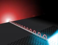 |
| Far-field photons excite silver nanowire plasmons. The wire plasmons propagate to the wire's distal end where they efficiently interact with the two-dimensional material semiconductor molybdenum disulfide (MoS2). The plasmons are absorbed in the MoS2 creating excitons that subsequently decay converting back into propagating photons.
Credit: Illustration by Michael Osadciw, Creative Services, University of Rochester |
Abstract:
A new combination of materials can efficiently guide electricity and light along the same tiny wire, a finding that could be a step towards building computer chips capable of transporting digital information at the speed of light.
Atomically thin material opens door for integrated nanophotonic circuits
Rochester, NY | Posted on September 4th, 2014Reporting today in The Optical Society's (OSA) high-impact journal Optica, optical and material scientists at the University of Rochester and Swiss Federal Institute of Technology in Zurich describe a basic model circuit consisting of a silver nanowire and a single-layer flake of molybendum disulfide (MoS2).
Using a laser to excite electromagnetic waves called plasmons at the surface of the wire, the researchers found that the MoS2 flake at the far end of the wire generated strong light emission. Going in the other direction, as the excited electrons relaxed, they were collected by the wire and converted back into plasmons, which emitted light of the same wavelength.
"We have found that there is pronounced nanoscale light-matter interaction between plasmons and atomically thin material that can be exploited for nanophotonic integrated circuits," said Nick Vamivakas, assistant professor of quantum optics and quantum physics at the University of Rochester and senior author of the paper.
Typically about a third of the remaining energy would be lost for every few microns (millionths of a meter) the plasmons traveled along the wire, explained Kenneth Goodfellow, a graduate student at Rochester's Institute of Optics and lead author of the Optica paper.
"It was surprising to see that enough energy was left after the round-trip," said Goodfellow.
Photonic devices can be much faster than electronic ones, but they are bulkier because devices that focus light cannot be miniaturized nearly as well as electronic circuits, said Goodfellow. The new results hold promise for guiding the transmission of light, and maintaining the intensity of the signal, in very small dimensions.
Ever since the discovery of graphene, a single layer of carbon that can be extracted from graphite with adhesive tape, scientists have been rapidly exploring the world of two-dimensional materials. These materials have unique properties not seen in their bulk form.
Like graphene, MoS2 is made up of layers that are weakly bonded to each other, so they can be easily separated. In bulk MoS2, electrons and photons interact as they would in traditional semiconductors like silicon and gallium arsenide. As MoS2 is reduced to thinner and thinner layers, the transfer of energy between electrons and photons becomes more efficient.
The key to MoS2's desirable photonic properties is in the structure of its energy band gap. As the material's layer count decreases, it transitions from an indirect to direct band gap, which allows electrons to easily move between energy bands by releasing photons. Graphene is inefficient at light emission because it has no band gap.
Combining electronics and photonics on the same integrated circuits could drastically improve the performance and efficiency of mobile technology. The researchers say the next step is to demonstrate their primitive circuit with light emitting diodes.
###
Paper: K. Goodfellow, R. Beams, C. Chakraborty, L. Novotny, A.N. Vamivakas "Integrated nanophotonics based on nanowire plasmons and atomically-thin material" Optica Vol. 1, Issue 3, pp.149-152 (2014).
####
About University of Rochester
The University of Rochester is one of the nation's leading private universities. Located in Rochester, N.Y., the University gives students exceptional opportunities for interdisciplinary study and close collaboration with faculty through its unique cluster-based curriculum. Its College, School of Arts and Sciences, and Hajim School of Engineering and Applied Sciences are complemented by its Eastman School of Music, Simon School of Business, Warner School of Education, Laboratory for Laser Energetics, School of Medicine and Dentistry, School of Nursing, Eastman Institute for Oral Health, and the Memorial Art Gallery.
For more information, please click here
Contacts:
David Barnstone
585-276-6264
Copyright © University of Rochester
If you have a comment, please Contact us.Issuers of news releases, not 7th Wave, Inc. or Nanotechnology Now, are solely responsible for the accuracy of the content.
Bookmark:


| Related News Press |
News and information
![]() Quantum computer improves AI predictions April 17th, 2026
Quantum computer improves AI predictions April 17th, 2026
![]() Flexible sensor gains sensitivity under pressure April 17th, 2026
Flexible sensor gains sensitivity under pressure April 17th, 2026
![]() A reusable chip for particulate matter sensing April 17th, 2026
A reusable chip for particulate matter sensing April 17th, 2026
![]() Detecting vibrational quantum beating in the predissociation dynamics of SF6 using time-resolved photoelectron spectroscopy April 17th, 2026
Detecting vibrational quantum beating in the predissociation dynamics of SF6 using time-resolved photoelectron spectroscopy April 17th, 2026
Chip Technology
![]() A reusable chip for particulate matter sensing April 17th, 2026
A reusable chip for particulate matter sensing April 17th, 2026
![]() Metasurfaces smooth light to boost magnetic sensing precision January 30th, 2026
Metasurfaces smooth light to boost magnetic sensing precision January 30th, 2026
Optical computing/Photonic computing
![]() ICFO researchers overcome long-standing bottleneck in single photon detection with twisted 2D materials August 8th, 2025
ICFO researchers overcome long-standing bottleneck in single photon detection with twisted 2D materials August 8th, 2025
![]() Programmable electron-induced color router array May 14th, 2025
Programmable electron-induced color router array May 14th, 2025
Discoveries
![]() Quantum computer improves AI predictions April 17th, 2026
Quantum computer improves AI predictions April 17th, 2026
![]() Flexible sensor gains sensitivity under pressure April 17th, 2026
Flexible sensor gains sensitivity under pressure April 17th, 2026
![]() A reusable chip for particulate matter sensing April 17th, 2026
A reusable chip for particulate matter sensing April 17th, 2026
![]() Detecting vibrational quantum beating in the predissociation dynamics of SF6 using time-resolved photoelectron spectroscopy April 17th, 2026
Detecting vibrational quantum beating in the predissociation dynamics of SF6 using time-resolved photoelectron spectroscopy April 17th, 2026
Announcements
![]() A fundamentally new therapeutic approach to cystic fibrosis: Nanobody repairs cellular defect April 17th, 2026
A fundamentally new therapeutic approach to cystic fibrosis: Nanobody repairs cellular defect April 17th, 2026
![]() UC Irvine physicists discover method to reverse �quantum scrambling� : The work addresses the problem of information loss in quantum computing system April 17th, 2026
UC Irvine physicists discover method to reverse �quantum scrambling� : The work addresses the problem of information loss in quantum computing system April 17th, 2026
Interviews/Book Reviews/Essays/Reports/Podcasts/Journals/White papers/Posters
![]() A fundamentally new therapeutic approach to cystic fibrosis: Nanobody repairs cellular defect April 17th, 2026
A fundamentally new therapeutic approach to cystic fibrosis: Nanobody repairs cellular defect April 17th, 2026
![]() UC Irvine physicists discover method to reverse �quantum scrambling� : The work addresses the problem of information loss in quantum computing system April 17th, 2026
UC Irvine physicists discover method to reverse �quantum scrambling� : The work addresses the problem of information loss in quantum computing system April 17th, 2026
Photonics/Optics/Lasers
![]() Metasurfaces smooth light to boost magnetic sensing precision January 30th, 2026
Metasurfaces smooth light to boost magnetic sensing precision January 30th, 2026
![]() From sensors to smart systems: the rise of AI-driven photonic noses January 30th, 2026
From sensors to smart systems: the rise of AI-driven photonic noses January 30th, 2026
|
|
||
|
|
||
| The latest news from around the world, FREE | ||
|
|
||
|
|
||
| Premium Products | ||
|
|
||
|
Only the news you want to read!
Learn More |
||
|
|
||
|
Full-service, expert consulting
Learn More |
||
|
|
||