Home > Press > Interlayer detector for ion beam milling processes
 |
Abstract:
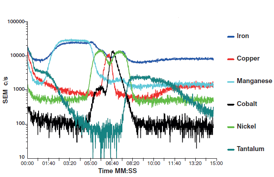
The Ion Beam Milling ion-etching process is vacuum based and is dependent on precise identification of interlayer breakthrough through multiple stacked thin-film layers each of perhaps only a few Angstrom thick . The Hiden IMP-EPD end point detector system is used routinely for monitoring and control of the total etching process. The system directly monitors the surface ions generated in the etching process, identifying the species present, their relative abundances and precisely defining the interlayer boundary to just 2.5 Angstrom. Species with molecular weights up to 300amu are determined.
Interlayer detector for ion beam milling processes
Warrington, UK | Posted on May 14th, 2014The IMP-EPD system is a differentially-pumped ruggedized secondary ion mass spectrometer used in both research and production process environments. Operation is fully automated with user adaptable programs enabling optimisation for the specific user process. Operation with full manual control is provided for the researcher and for service/maintenance functions.
Additionally to end-point analysis the system operates as a highly sensitive residual gas analyser for measurement of system background gases, and for leak detection with user choice of search gas.
For full details of the system, and of other Hiden surface analysis tools, please contact Hiden Analytical at or visit the main website at www.HidenAnalytical.com.
####
For more information, please click here
Contacts:
Jessica Neale
Marketing Administrator
T +44(0)1925 445225
F +44(0)1925 416518
Copyright © Hiden Analytical Ltd
If you have a comment, please Contact us.Issuers of news releases, not 7th Wave, Inc. or Nanotechnology Now, are solely responsible for the accuracy of the content.
| Related News Press |
News and information
![]() Quantum computer improves AI predictions April 17th, 2026
Quantum computer improves AI predictions April 17th, 2026
![]() Flexible sensor gains sensitivity under pressure April 17th, 2026
Flexible sensor gains sensitivity under pressure April 17th, 2026
![]() A reusable chip for particulate matter sensing April 17th, 2026
A reusable chip for particulate matter sensing April 17th, 2026
![]() Detecting vibrational quantum beating in the predissociation dynamics of SF6 using time-resolved photoelectron spectroscopy April 17th, 2026
Detecting vibrational quantum beating in the predissociation dynamics of SF6 using time-resolved photoelectron spectroscopy April 17th, 2026
Announcements
![]() A fundamentally new therapeutic approach to cystic fibrosis: Nanobody repairs cellular defect April 17th, 2026
A fundamentally new therapeutic approach to cystic fibrosis: Nanobody repairs cellular defect April 17th, 2026
![]() UC Irvine physicists discover method to reverse �quantum scrambling� : The work addresses the problem of information loss in quantum computing system April 17th, 2026
UC Irvine physicists discover method to reverse �quantum scrambling� : The work addresses the problem of information loss in quantum computing system April 17th, 2026
Tools
![]() Metasurfaces smooth light to boost magnetic sensing precision January 30th, 2026
Metasurfaces smooth light to boost magnetic sensing precision January 30th, 2026
![]() From sensors to smart systems: the rise of AI-driven photonic noses January 30th, 2026
From sensors to smart systems: the rise of AI-driven photonic noses January 30th, 2026
![]() Japan launches fully domestically produced quantum computer: Expo visitors to experience quantum computing firsthand August 8th, 2025
Japan launches fully domestically produced quantum computer: Expo visitors to experience quantum computing firsthand August 8th, 2025
|
|
||
|
|
||
| The latest news from around the world, FREE | ||
|
|
||
|
|
||
| Premium Products | ||
|
|
||
|
Only the news you want to read!
Learn More |
||
|
|
||
|
Full-service, expert consulting
Learn More |
||
|
|
||


