Home > Press > Atomic switcheroo explains origins of thin-film solar cell mystery
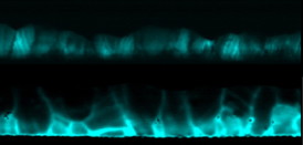 |
| Cross-sectional electron beam-induced current maps show the difference in cadmium telluride solar cells before (pictured above) and after (below) cadmium chloride treatment. The increased brightness after treatment indicates higher current collection at the grain boundaries. |
Abstract:
Treating cadmium-telluride (CdTe) solar cell materials with cadmium-chloride improves their efficiency, but researchers have not fully understood why. Now, an atomic-scale examination of the thin-film solar cells led by the Department of Energy's Oak Ridge National Laboratory has answered this decades-long debate about the materials' photovoltaic efficiency increase after treatment.
Atomic switcheroo explains origins of thin-film solar cell mystery
Oak Ridge, TN | Posted on April 23rd, 2014 A research team from ORNL, the University of Toledo and DOE's National Renewable Energy Laboratory used electron microscopy and computational simulations to explore the physical origins of the unexplained treatment process. The results are published in Physical Review Letters (PRL).
Thin-film CdTe solar cells are considered a potential rival to silicon-based photovoltaic systems because of their theoretically low cost per power output and ease of fabrication. Their comparatively low historical efficiency in converting sunlight into energy, however, has limited the technology's widespread use, especially for home systems.
Research in the 1980s showed that treating CdTe thin films with cadmium-chloride significantly raises the cell's efficiency, but scientists have been unable to determine the underlying causes. ORNL's Chen Li, first author on the PRL study, explains that the answer lay in investigating the material at an atomic level.
"We knew that chlorine was responsible for this magical effect, but we needed to find out where it went in the material's structure," Li said. "Only by understanding the structure can we understand what's wrong in this solar cell -- why the efficiency is not high enough, and how can we push it further."
By comparing the solar cells before and after chlorine treatment, the researchers realized that atom-scale grain boundaries were implicated in the enhanced performance. Grain boundaries are tiny defects that that normally act as roadblocks to efficiency, because they inhibit carrier collection which greatly reduces the solar cell power.
Using state of the art electron microscopy techniques to study the thin films' structure and chemical composition after treatment, the researchers found that chlorine atoms replaced tellurium atoms within the grain boundaries. This atomic substitution creates local electric fields at the grain boundaries that boost the material's photovoltaic performance instead of damaging it.
The research team's finding, in addition to providing a long-awaited explanation, could be used to guide engineering of higher-efficiency CdTe solar cells. Controlling the grain boundary structure, says Li, is a new direction that could help raise the cell efficiencies closer to the theoretical maximum of 32 percent light-to-energy conversion. Currently, the record CdTe cell efficiency is only 20.4 percent.
"We think that if all the grain boundaries in a thin film material could be aligned in same direction, it could improve cell efficiency even further," Li said.
The team's research appears as "Grain-Boundary-Enhanced Carrier Collection in CdTe Solar Cells." Coauthors are ORNL's Chen Li, Jonathan Poplawsky, Mark Oxley and Andrew Lupini; University of Toledo's Yelong Wu, Naba Paudel, Wanjian Yin and Yanfa Yan; University of Tennessee's Stephen Pennycook; University of Manchester's Sarah Haigh; University of Oxford's Timothy Pennycook; and NREL's Mowafak Al-Jassim. Li and Oxley hold joint appointments at Vanderbilt University.
The research was supported by the Department of Energy's Office of Energy Efficiency and Renewable Energy through the SunShot Initiative and the Office of Basic Energy Sciences. The work was sponsored in part by the UK Engineering and Physical Sciences Research Council and through a user project supported by ORNL's Center for Nanophase Materials Sciences (CNMS). This research used resources of the National Energy Research Scientific Computing Center. Yan acknowledges support from the Ohio Research Scholar Program.
CNMS is one of the five DOE Nanoscale Science Research Centers, NSRCs, supported by the DOE Office of Science, as premier national user facilities for interdisciplinary research at the nanoscale. Together the NSRCs comprise a suite of complementary facilities that provide researchers with state-of-the-art capabilities to fabricate, process, characterize and model nanoscale materials, and constitute the largest infrastructure investment of the National Nanotechnology Initiative. The NSRCs are located at DOE's Argonne, Brookhaven, Lawrence Berkeley, Oak Ridge and Sandia and Los Alamos national laboratories. For more information about the DOE NSRCs, please visit http://science.energy.gov/bes/suf/user-facilities/nanoscale-science-research-centers/.
####
About DOE/Oak Ridge National Laboratory
ORNL is managed by UT-Battelle for the Department of Energy's Office of Science.
DOE�s Office of Science is the single largest supporter of basic research in the physical sciences in the United States, and is working to address some of the most pressing challenges of our time. For more information, please visit science.energy.gov.
For more information, please click here
Contacts:
Morgan McCorkle
865-574-7308
Copyright © DOE/Oak Ridge National Laboratory
If you have a comment, please Contact us.Issuers of news releases, not 7th Wave, Inc. or Nanotechnology Now, are solely responsible for the accuracy of the content.
Bookmark:


| Related News Press |
News and information
![]() Quantum computer improves AI predictions April 17th, 2026
Quantum computer improves AI predictions April 17th, 2026
![]() Flexible sensor gains sensitivity under pressure April 17th, 2026
Flexible sensor gains sensitivity under pressure April 17th, 2026
![]() A reusable chip for particulate matter sensing April 17th, 2026
A reusable chip for particulate matter sensing April 17th, 2026
![]() Detecting vibrational quantum beating in the predissociation dynamics of SF6 using time-resolved photoelectron spectroscopy April 17th, 2026
Detecting vibrational quantum beating in the predissociation dynamics of SF6 using time-resolved photoelectron spectroscopy April 17th, 2026
Thin films
![]() Tiny nanosheets, big leap: A new sensor detects ethanol at ultra-low levels January 30th, 2026
Tiny nanosheets, big leap: A new sensor detects ethanol at ultra-low levels January 30th, 2026
![]() Utilizing palladium for addressing contact issues of buried oxide thin film transistors April 5th, 2024
Utilizing palladium for addressing contact issues of buried oxide thin film transistors April 5th, 2024
Laboratories
![]() Researchers develop molecular qubits that communicate at telecom frequencies October 3rd, 2025
Researchers develop molecular qubits that communicate at telecom frequencies October 3rd, 2025
Govt.-Legislation/Regulation/Funding/Policy
![]() Quantum computer improves AI predictions April 17th, 2026
Quantum computer improves AI predictions April 17th, 2026
![]() Metasurfaces smooth light to boost magnetic sensing precision January 30th, 2026
Metasurfaces smooth light to boost magnetic sensing precision January 30th, 2026
![]() New imaging approach transforms study of bacterial biofilms August 8th, 2025
New imaging approach transforms study of bacterial biofilms August 8th, 2025
Discoveries
![]() Quantum computer improves AI predictions April 17th, 2026
Quantum computer improves AI predictions April 17th, 2026
![]() Flexible sensor gains sensitivity under pressure April 17th, 2026
Flexible sensor gains sensitivity under pressure April 17th, 2026
![]() A reusable chip for particulate matter sensing April 17th, 2026
A reusable chip for particulate matter sensing April 17th, 2026
![]() Detecting vibrational quantum beating in the predissociation dynamics of SF6 using time-resolved photoelectron spectroscopy April 17th, 2026
Detecting vibrational quantum beating in the predissociation dynamics of SF6 using time-resolved photoelectron spectroscopy April 17th, 2026
Announcements
![]() A fundamentally new therapeutic approach to cystic fibrosis: Nanobody repairs cellular defect April 17th, 2026
A fundamentally new therapeutic approach to cystic fibrosis: Nanobody repairs cellular defect April 17th, 2026
![]() UC Irvine physicists discover method to reverse �quantum scrambling� : The work addresses the problem of information loss in quantum computing system April 17th, 2026
UC Irvine physicists discover method to reverse �quantum scrambling� : The work addresses the problem of information loss in quantum computing system April 17th, 2026
Energy
![]() Sensors innovations for smart lithium-based batteries: advancements, opportunities, and potential challenges August 8th, 2025
Sensors innovations for smart lithium-based batteries: advancements, opportunities, and potential challenges August 8th, 2025
![]() Simple algorithm paired with standard imaging tool could predict failure in lithium metal batteries August 8th, 2025
Simple algorithm paired with standard imaging tool could predict failure in lithium metal batteries August 8th, 2025
Solar/Photovoltaic
![]() Spinel-type sulfide semiconductors to operate the next-generation LEDs and solar cells For solar-cell absorbers and green-LED source October 3rd, 2025
Spinel-type sulfide semiconductors to operate the next-generation LEDs and solar cells For solar-cell absorbers and green-LED source October 3rd, 2025
![]() KAIST researchers introduce new and improved, next-generation perovskite solar cell November 8th, 2024
KAIST researchers introduce new and improved, next-generation perovskite solar cell November 8th, 2024
![]() Groundbreaking precision in single-molecule optoelectronics August 16th, 2024
Groundbreaking precision in single-molecule optoelectronics August 16th, 2024
![]() Development of zinc oxide nanopagoda array photoelectrode: photoelectrochemical water-splitting hydrogen production January 12th, 2024
Development of zinc oxide nanopagoda array photoelectrode: photoelectrochemical water-splitting hydrogen production January 12th, 2024
|
|
||
|
|
||
| The latest news from around the world, FREE | ||
|
|
||
|
|
||
| Premium Products | ||
|
|
||
|
Only the news you want to read!
Learn More |
||
|
|
||
|
Full-service, expert consulting
Learn More |
||
|
|
||