Home > Press > Fabricating Nanostructures with Silk Could Make Clean Rooms Green Rooms
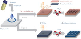 |
| Above: Optical-grade silk fibroin aqueous solution, obtained from the cocoons of the Bombyx mori caterpillar, was placed on a substrate and spin-coated to form a silk film. Both positive and negative resists were formed and developed using water. |
Abstract:
Tufts University engineers have demonstrated that it is possible to generate nanostructures from silk in an environmentally friendly process that uses water as a developing agent and standard fabrication techniques. This approach provides a green alternative to the toxic materials commonly used in nanofabrication while delivering fabrication quality comparable to conventional synthetic polymers. Nanofabrication is at the heart of manufacture of semi-conductors and other electronic and photonic devices.
Fabricating Nanostructures with Silk Could Make Clean Rooms Green Rooms
Medford/Sumerville, MA | Posted on March 31st, 2014The paper describing this work, "All Water-based Electron Beam Lithography Using Silk as a Positive, Negative and Biofunctional Resist," appears in Nature Nanotechnology, published online March 23 in advance of print publication.
"In a world that strives to reduce toxic footprints associated with manufacturing, our laboratory is exploring biopolymers, and silk in particular, as a candidate material to replace plastics in many high-technology applications," said Frank C. Doble Professor of Biomedical Engineering Fiorenzo Omenetto, Ph.D., senior researcher on the work.
Nanofabrication involves high-resolution patterning with features so small that they have at least one dimension no larger than 100 nanometers (nm)�the size of particles filtered out by surgical masks. Nanoscale fabrication is usually obtained depositing thin films of customized polymers, called "resists," onto silicon wafers. Each resist layer is successively patterned by using light or electrons (via electron beam lithography) to expose the part of the resist not covered by a mask. Subsequently, positive resists are dissolved when subjected to a developer while negative resists remain behind after development. The composition and configuration of the layers determine the properties of the structure.
Developing a resist typically requires toxic chemicals, which need careful, and costly, handling and disposal. Significant advances have been made using "green" resists that can be developed with water, but these techniques have lacked the desired precision and scalability.
"In contrast, our process is entirely water-based, starting with the silk aqueous solution and ending with simple development of the exposed silk film in water, and the resolution achieved was comparable to one of the commonly used synthetic polymers," said Omenetto, who holds a professorship in the Department of Physics at Tufts School of Arts and Sciences in addition to his appointment in the School of Engineering. "A variety of manufacturing industries, high-tech companies and academic labs could ultimately benefit from clean rooms that are also green."
For this work, the Tufts engineers fabricated nanoscale photonic lattices using both neat silk and functionalized silk doped with quantum dots, green fluorescent proteins (GFPs) or horseradish peroxidase (HRP).
"By showing that biomolecules of the enzyme HRP remained active after the electron beam nanofabrication process, we demonstrated the feasibility of fabricating biologically active silk sensing devices, something not currently available," said Benedetto Marelli, Ph.D. Marelli is a post-doctoral associate in Omenetto's laboratory and a lead co-author on the paper with former Omenetto post doctoral associate Sunghwan Kim, Ph.D., now a professor in Ajou, Korea.
This research builds on previous work by Omenetto and his collaborators at the Tufts School of Engineering. In the past, they had shown that silk could be nanofabricated, but those processes required starting with other nanosized materials. This is the first time that silk has been fabricated to begin the nanofabrication manufacturing chain.
The work was supported by the National Science Foundation (DMR-1242240), ONR (N00014-13-1-0596) and AFOSR (FA9950-10-1-0172).
"All-water-based electron-beam lithography using silk as a resist," Sunghwan Kim, Benedetto Marelli, Mark A. Brenckle, Alexander N. Mitropoulos, Eun-Seok Gil, Konstantinos Tsioris, Hu Tao, David L. Kaplan, & Fiorenzo G. Omenetto, Nature Nanotechnology, doi:10.1038/nnano.2014.47, published online 23 March 2014.
####
About Tufts University
Located on Tufts� Medford/Somerville campus, the Tufts University School of Engineering offers a rigorous engineering education in a unique environment that blends the intellectual and technological resources of a world-class research university with the strengths of a top-ranked liberal arts college. Close partnerships with Tufts� excellent undergraduate, graduate and professional schools, coupled with a long tradition of collaboration, provide a strong platform for interdisciplinary education and scholarship. The School of Engineering�s mission is to educate engineers committed to the innovative and ethical application of science and technology in addressing the most pressing societal needs, to develop and nurture twenty-first century leadership qualities in its students, faculty, and alumni, and to create and disseminate transformational new knowledge and technologies that further the well-being and sustainability of society in such cross-cutting areas as human health, environmental sustainability, alternative energy, and the human-technology interface. For more information, visit engineering.tufts.edu.
For more information, please click here
Contacts:
Kim Thurler
617.627.3175
Copyright © Tufts University
If you have a comment, please Contact us.Issuers of news releases, not 7th Wave, Inc. or Nanotechnology Now, are solely responsible for the accuracy of the content.
Bookmark:


| Related Links |
![]() Biomedical Engineering at Tufts:
Biomedical Engineering at Tufts:
| Related News Press |
News and information
![]() Quantum computer improves AI predictions April 17th, 2026
Quantum computer improves AI predictions April 17th, 2026
![]() Flexible sensor gains sensitivity under pressure April 17th, 2026
Flexible sensor gains sensitivity under pressure April 17th, 2026
![]() A reusable chip for particulate matter sensing April 17th, 2026
A reusable chip for particulate matter sensing April 17th, 2026
![]() Detecting vibrational quantum beating in the predissociation dynamics of SF6 using time-resolved photoelectron spectroscopy April 17th, 2026
Detecting vibrational quantum beating in the predissociation dynamics of SF6 using time-resolved photoelectron spectroscopy April 17th, 2026
Chip Technology
![]() A reusable chip for particulate matter sensing April 17th, 2026
A reusable chip for particulate matter sensing April 17th, 2026
![]() Metasurfaces smooth light to boost magnetic sensing precision January 30th, 2026
Metasurfaces smooth light to boost magnetic sensing precision January 30th, 2026
Discoveries
![]() Quantum computer improves AI predictions April 17th, 2026
Quantum computer improves AI predictions April 17th, 2026
![]() Flexible sensor gains sensitivity under pressure April 17th, 2026
Flexible sensor gains sensitivity under pressure April 17th, 2026
![]() A reusable chip for particulate matter sensing April 17th, 2026
A reusable chip for particulate matter sensing April 17th, 2026
![]() Detecting vibrational quantum beating in the predissociation dynamics of SF6 using time-resolved photoelectron spectroscopy April 17th, 2026
Detecting vibrational quantum beating in the predissociation dynamics of SF6 using time-resolved photoelectron spectroscopy April 17th, 2026
Materials/Metamaterials/Magnetoresistance
![]() First real-time observation of two-dimensional melting process: Researchers at Mainz University unveil new insights into magnetic vortex structures August 8th, 2025
First real-time observation of two-dimensional melting process: Researchers at Mainz University unveil new insights into magnetic vortex structures August 8th, 2025
![]() Researchers unveil a groundbreaking clay-based solution to capture carbon dioxide and combat climate change June 6th, 2025
Researchers unveil a groundbreaking clay-based solution to capture carbon dioxide and combat climate change June 6th, 2025
![]() A 1960s idea inspires NBI researchers to study hitherto inaccessible quantum states June 6th, 2025
A 1960s idea inspires NBI researchers to study hitherto inaccessible quantum states June 6th, 2025
![]() Institute for Nanoscience hosts annual proposal planning meeting May 16th, 2025
Institute for Nanoscience hosts annual proposal planning meeting May 16th, 2025
Announcements
![]() A fundamentally new therapeutic approach to cystic fibrosis: Nanobody repairs cellular defect April 17th, 2026
A fundamentally new therapeutic approach to cystic fibrosis: Nanobody repairs cellular defect April 17th, 2026
![]() UC Irvine physicists discover method to reverse �quantum scrambling� : The work addresses the problem of information loss in quantum computing system April 17th, 2026
UC Irvine physicists discover method to reverse �quantum scrambling� : The work addresses the problem of information loss in quantum computing system April 17th, 2026
Interviews/Book Reviews/Essays/Reports/Podcasts/Journals/White papers/Posters
![]() A fundamentally new therapeutic approach to cystic fibrosis: Nanobody repairs cellular defect April 17th, 2026
A fundamentally new therapeutic approach to cystic fibrosis: Nanobody repairs cellular defect April 17th, 2026
![]() UC Irvine physicists discover method to reverse �quantum scrambling� : The work addresses the problem of information loss in quantum computing system April 17th, 2026
UC Irvine physicists discover method to reverse �quantum scrambling� : The work addresses the problem of information loss in quantum computing system April 17th, 2026
Environment
![]() A reusable chip for particulate matter sensing April 17th, 2026
A reusable chip for particulate matter sensing April 17th, 2026
![]() Researchers unveil a groundbreaking clay-based solution to capture carbon dioxide and combat climate change June 6th, 2025
Researchers unveil a groundbreaking clay-based solution to capture carbon dioxide and combat climate change June 6th, 2025
Photonics/Optics/Lasers
![]() Metasurfaces smooth light to boost magnetic sensing precision January 30th, 2026
Metasurfaces smooth light to boost magnetic sensing precision January 30th, 2026
![]() From sensors to smart systems: the rise of AI-driven photonic noses January 30th, 2026
From sensors to smart systems: the rise of AI-driven photonic noses January 30th, 2026
|
|
||
|
|
||
| The latest news from around the world, FREE | ||
|
|
||
|
|
||
| Premium Products | ||
|
|
||
|
Only the news you want to read!
Learn More |
||
|
|
||
|
Full-service, expert consulting
Learn More |
||
|
|
||