Home > Press > Rainbow-catching waveguide could revolutionize energy technologies: By slowing and absorbing certain wavelengths of light, engineers open new possibilities in solar power, thermal energy recycling and stealth technology
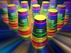 |
| The image shows a �multilayered waveguide taper array.� The different wavelengths, or colors, are absorbed by the waveguide tapers (thimble-shaped structures) that together form an array. |
Abstract:
More efficient photovoltaic cells. Improved radar and stealth technology. A new way to recycle waste heat generated by machines into energy.
Rainbow-catching waveguide could revolutionize energy technologies: By slowing and absorbing certain wavelengths of light, engineers open new possibilities in solar power, thermal energy recycling and stealth technology
Buffalo, NY | Posted on March 28th, 2014All may be possible due to breakthrough photonics research at the University at Buffalo.
The work, published March 28 in the journal Scientific Reports, explores the use of a nanoscale microchip component called a "multilayered waveguide taper array" that improves the chip's ability to trap and absorb light.
Unlike current chips, the waveguide tapers (the thimble-shaped structures pictured above) slow and ultimately absorb each frequency of light at different places vertically to catch a "rainbow" of wavelengths, or broadband light.
The paper, "Broadband absorption engineering of hyperbolic metafilm patterns," is here: http://bit.ly/1g72Is5.
"We previously predicted the multilayered waveguide tapers would more efficiently absorb light, and now we've proved it with these experiments," says lead researcher Qiaoqiang Gan, PhD, UB assistant professor of electrical engineering. "This advancement could prove invaluable for thin-film solar technology, as well as recycling waste thermal energy that is a byproduct of industry and everyday electronic devices such as smartphones and laptops."
Each multilayered waveguide taper is made of ultrathin layers of metal, semiconductors and/or insulators. The tapers absorb light in metal dielectric layer pairs, the so-called hyperbolic metamaterial. By adjusting the thickness of the layers and other geometric parameters, the tapers can be tuned to different frequencies including visible, near-infrared, mid-infrared, terahertz and microwaves.
The structure could lead to advancements in an array of fields.
For example, there is a relatively new field of advanced computing research called on-chip optical communication. In this field, there is a phenomenon known as crosstalk, in which an optical signal transmitted on one waveguide channel creates an undesired scattering or coupling effect on another waveguide channel. The multilayered waveguide taper structure array could potentially prevent this.
It could also improve thin-film photovoltaic cells, which are a promising because they are less expensive and more flexible that traditional solar cells. The drawback, however, is that they don't absorb as much light as traditional cells. Because the multilayered waveguide taper structure array can efficiently absorb the visible spectrum, as well as the infrared spectrum, it could potentially boost the amount of energy that thin-film solar cells generate.
The multilayered waveguide taper array could help recycle waste heat generated by power plants and other industrial processes, as well as electronic devices such as televisions, smartphones and laptop computers.
"It could be useful as an ultra compact thermal-absorption, collection and liberation device in the mid-infrared spectrum," says Dengxin Ji, a PhD student in Gan's lab and first author of the paper.
It could even be used as a stealth, or cloaking, material for airplanes, ships and other vehicles to avoid radar, sonar, infrared and other forms of detection. "The multilayered waveguide tapers can be scaled up to tune the absorption band to a lower frequency domain and absorb microwaves efficiently," says Haomin Song, another PhD student in Gan's lab and the paper's second author.
Additional authors of the paper include Haifeng Hu, Kai Liu, Xie Zeng and Nan Zhang, all PhD candidates in UB's Department of Electrical Engineering.
The National Science Foundation sponsored the research.
Gan is a member of UB's electrical engineering optics and photonics research group, which includes professors Alexander N. Cartwright (also UB vice president for research and economic development), Edward Furlani and Pao-Lo Liu; associate professor Natalia Litchinitser; and assistant professor Liang Feng.
The group carries out research in nanophotonics, biophotonics, hybrid inorganic/organic materials and devices, nonlinear and fiber optics, metamaterials, nanoplasmonics, optofluidics, microelectromechanical systems (MEMS), biomedical microelectromechanical systems (BioMEMs), biosensing and quantum information processing.
####
For more information, please click here
Contacts:
Cory Nealon
Media Relations Manager, Engineering, Libraries, Sustainability
Tel: 716-645-4614
Copyright © University at Buffalo
If you have a comment, please Contact us.Issuers of news releases, not 7th Wave, Inc. or Nanotechnology Now, are solely responsible for the accuracy of the content.
Bookmark:


| Related News Press |
News and information
![]() Quantum computer improves AI predictions April 17th, 2026
Quantum computer improves AI predictions April 17th, 2026
![]() Flexible sensor gains sensitivity under pressure April 17th, 2026
Flexible sensor gains sensitivity under pressure April 17th, 2026
![]() A reusable chip for particulate matter sensing April 17th, 2026
A reusable chip for particulate matter sensing April 17th, 2026
![]() Detecting vibrational quantum beating in the predissociation dynamics of SF6 using time-resolved photoelectron spectroscopy April 17th, 2026
Detecting vibrational quantum beating in the predissociation dynamics of SF6 using time-resolved photoelectron spectroscopy April 17th, 2026
Govt.-Legislation/Regulation/Funding/Policy
![]() Quantum computer improves AI predictions April 17th, 2026
Quantum computer improves AI predictions April 17th, 2026
![]() Metasurfaces smooth light to boost magnetic sensing precision January 30th, 2026
Metasurfaces smooth light to boost magnetic sensing precision January 30th, 2026
![]() New imaging approach transforms study of bacterial biofilms August 8th, 2025
New imaging approach transforms study of bacterial biofilms August 8th, 2025
MEMS
Quantum Computing
![]() Quantum computer improves AI predictions April 17th, 2026
Quantum computer improves AI predictions April 17th, 2026
![]() UC Irvine physicists discover method to reverse �quantum scrambling� : The work addresses the problem of information loss in quantum computing system April 17th, 2026
UC Irvine physicists discover method to reverse �quantum scrambling� : The work addresses the problem of information loss in quantum computing system April 17th, 2026
![]() Researchers develop molecular qubits that communicate at telecom frequencies October 3rd, 2025
Researchers develop molecular qubits that communicate at telecom frequencies October 3rd, 2025
Discoveries
![]() Quantum computer improves AI predictions April 17th, 2026
Quantum computer improves AI predictions April 17th, 2026
![]() Flexible sensor gains sensitivity under pressure April 17th, 2026
Flexible sensor gains sensitivity under pressure April 17th, 2026
![]() A reusable chip for particulate matter sensing April 17th, 2026
A reusable chip for particulate matter sensing April 17th, 2026
![]() Detecting vibrational quantum beating in the predissociation dynamics of SF6 using time-resolved photoelectron spectroscopy April 17th, 2026
Detecting vibrational quantum beating in the predissociation dynamics of SF6 using time-resolved photoelectron spectroscopy April 17th, 2026
Announcements
![]() A fundamentally new therapeutic approach to cystic fibrosis: Nanobody repairs cellular defect April 17th, 2026
A fundamentally new therapeutic approach to cystic fibrosis: Nanobody repairs cellular defect April 17th, 2026
![]() UC Irvine physicists discover method to reverse �quantum scrambling� : The work addresses the problem of information loss in quantum computing system April 17th, 2026
UC Irvine physicists discover method to reverse �quantum scrambling� : The work addresses the problem of information loss in quantum computing system April 17th, 2026
Military
![]() Quantum engineers �squeeze� laser frequency combs to make more sensitive gas sensors January 17th, 2025
Quantum engineers �squeeze� laser frequency combs to make more sensitive gas sensors January 17th, 2025
![]() Chainmail-like material could be the future of armor: First 2D mechanically interlocked polymer exhibits exceptional flexibility and strength January 17th, 2025
Chainmail-like material could be the future of armor: First 2D mechanically interlocked polymer exhibits exceptional flexibility and strength January 17th, 2025
![]() Single atoms show their true color July 5th, 2024
Single atoms show their true color July 5th, 2024
![]() NRL charters Navy�s quantum inertial navigation path to reduce drift April 5th, 2024
NRL charters Navy�s quantum inertial navigation path to reduce drift April 5th, 2024
Energy
![]() Sensors innovations for smart lithium-based batteries: advancements, opportunities, and potential challenges August 8th, 2025
Sensors innovations for smart lithium-based batteries: advancements, opportunities, and potential challenges August 8th, 2025
![]() Simple algorithm paired with standard imaging tool could predict failure in lithium metal batteries August 8th, 2025
Simple algorithm paired with standard imaging tool could predict failure in lithium metal batteries August 8th, 2025
Photonics/Optics/Lasers
![]() Metasurfaces smooth light to boost magnetic sensing precision January 30th, 2026
Metasurfaces smooth light to boost magnetic sensing precision January 30th, 2026
![]() From sensors to smart systems: the rise of AI-driven photonic noses January 30th, 2026
From sensors to smart systems: the rise of AI-driven photonic noses January 30th, 2026
Solar/Photovoltaic
![]() Spinel-type sulfide semiconductors to operate the next-generation LEDs and solar cells For solar-cell absorbers and green-LED source October 3rd, 2025
Spinel-type sulfide semiconductors to operate the next-generation LEDs and solar cells For solar-cell absorbers and green-LED source October 3rd, 2025
![]() KAIST researchers introduce new and improved, next-generation perovskite solar cell November 8th, 2024
KAIST researchers introduce new and improved, next-generation perovskite solar cell November 8th, 2024
![]() Groundbreaking precision in single-molecule optoelectronics August 16th, 2024
Groundbreaking precision in single-molecule optoelectronics August 16th, 2024
![]() Development of zinc oxide nanopagoda array photoelectrode: photoelectrochemical water-splitting hydrogen production January 12th, 2024
Development of zinc oxide nanopagoda array photoelectrode: photoelectrochemical water-splitting hydrogen production January 12th, 2024
|
|
||
|
|
||
| The latest news from around the world, FREE | ||
|
|
||
|
|
||
| Premium Products | ||
|
|
||
|
Only the news you want to read!
Learn More |
||
|
|
||
|
Full-service, expert consulting
Learn More |
||
|
|
||