Home > Press > A new concept for manufacturing wrinkling patterns on hard-nano-film/soft-matter-substrate
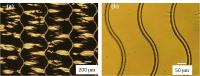 |
| This image shows a set of S-shaped curves with the same phase. (a) The parallel distance 800 μm; (b) the parallel distance 200 μm (aluminum film thickness 200 nm).
Credit: �Science China Press |
Abstract:
Wrinkling is a common phenomenon for thin stiff film adhered on soft substrate. Various wrinkling phenomenon has been reported previously. Wu Dan, Yin Yajun, Xie Huimin,et al from Tsinghua University proposed a new method to control wrinkling and buckling of thin stiff film on soft substrate. It is found that the curve pattern on the soft substrate has obvious influence on the wrinkling distribution of the thin film/soft substrate. Their work, entitled "Controlling the surface buckling wrinkles by patterning the material system of hard-nano-film/soft-matter-substrate", was published in SCIENCE CHINA Physics, Mechanics & Astronomy 2014, Vol 57(4) issue.
A new concept for manufacturing wrinkling patterns on hard-nano-film/soft-matter-substrate
Beijing, China | Posted on March 24th, 2014Wrinkling and buckling at micro-scale are a popular phenomenon in stiff nano-film on compliant substrate due to external stimuli such as thermal mismatch. This feature has many applications in the design and fabrication of flexible electronics and devices, micro-cell arrays, optical gratings, and so on.
Thermal mismatch is one of the important factors which cause the surface buckling of stiff nano-film on compliant substrate. The wrinkling formation mechanism of the stiff film on compliant substrate of Polydimethylsiloxane (PDMS) is illustrated in Figure 1. The PDMS substrate is heated and will be expanded as a result during the deposition of the stiff film. When the deposition is completed, the stiff film is formed on the substrate and the substrate cools down. The contraction of the substrate due to temperature dropping is restricted by the stiff film, for the thermal coefficient of the PDMS substrate is much larger than the stiff film. In accommodating the deformation mismatch between the substrate and the stiff film, interface constraint force is induced consequently. The deformation compatibility causes compressive stress in the stiff film and tensile stress in the compliant PDMS substrate. Once the compressive stress in the stiff film exceeds the critical buckling stress, surface buckling and wrinkling will occur to balance the system.
The wrinkling appears randomly and in disorder in the uniform, continuous and isotropic film under the condition of equally biaxial compressive stress. The orientation ordering of wrinkles induced by isotropic buckling has been studied by simulation method but few works have been reported on how to control the surface wrinkling orientation according to the design specification, which is significant for the design of the flexible electronics. The idea of regulating the orientation and distribution of the wrinkling by patterning the surface of the stiff film/compliant substrate system has been proposed by researchers recently. Various patterns have been designed on the PDMS substrate to control the buckling distribution and orientation. Some progress from recent work has been made in this research.
A photolithography process has been conducted to fabricate the curve patterns on the soft PDMS substrate and then the thin stiff aluminum film is deposited on the soft substrate. A few experimental results have been show in Figure 2 and Figure 3. Through the wrinkling behavior of the thin stiff film/soft substrate by patterning the soft substrate with various curves, the conclusions are summarized: On the concave side of the curve, the wrinkling of the film surface is suppressed to be identified as shielding effect and on the convex side the wrinkling of the film surface is induced to be identified as inductive effect. The shielding and inductive effects make the dis-ordered wrinkling and buckling controllable. This finding may give some new ideas to the designing of the wrinkling pattern of thin stiff film/soft substrate.
####
About Science China Press
Science China Press Co., Ltd. (SCP) is a scientific journal publishing company of the Chinese Academy of Sciences (CAS). For 60 years, SCP takes its mission to present to the world the best achievements by Chinese scientists on various fields of natural sciences researches.
For more information, please click here
Contacts:
Xie Huimin
Copyright © Science China Press
If you have a comment, please Contact us.Issuers of news releases, not 7th Wave, Inc. or Nanotechnology Now, are solely responsible for the accuracy of the content.
Bookmark:


| Related Links |
| Related News Press |
News and information
![]() Quantum computer improves AI predictions April 17th, 2026
Quantum computer improves AI predictions April 17th, 2026
![]() Flexible sensor gains sensitivity under pressure April 17th, 2026
Flexible sensor gains sensitivity under pressure April 17th, 2026
![]() A reusable chip for particulate matter sensing April 17th, 2026
A reusable chip for particulate matter sensing April 17th, 2026
![]() Detecting vibrational quantum beating in the predissociation dynamics of SF6 using time-resolved photoelectron spectroscopy April 17th, 2026
Detecting vibrational quantum beating in the predissociation dynamics of SF6 using time-resolved photoelectron spectroscopy April 17th, 2026
Flexible Electronics
![]() Flexible sensor gains sensitivity under pressure April 17th, 2026
Flexible sensor gains sensitivity under pressure April 17th, 2026
![]() MXene nanomaterials enter a new dimension Multilayer nanomaterial: MXene flakes created at Drexel University show new promise as 1D scrolls January 30th, 2026
MXene nanomaterials enter a new dimension Multilayer nanomaterial: MXene flakes created at Drexel University show new promise as 1D scrolls January 30th, 2026
![]() Flexible electronics integrated with paper-thin structure for use in space January 17th, 2025
Flexible electronics integrated with paper-thin structure for use in space January 17th, 2025
Thin films
![]() Tiny nanosheets, big leap: A new sensor detects ethanol at ultra-low levels January 30th, 2026
Tiny nanosheets, big leap: A new sensor detects ethanol at ultra-low levels January 30th, 2026
Discoveries
![]() Quantum computer improves AI predictions April 17th, 2026
Quantum computer improves AI predictions April 17th, 2026
![]() Flexible sensor gains sensitivity under pressure April 17th, 2026
Flexible sensor gains sensitivity under pressure April 17th, 2026
![]() A reusable chip for particulate matter sensing April 17th, 2026
A reusable chip for particulate matter sensing April 17th, 2026
![]() Detecting vibrational quantum beating in the predissociation dynamics of SF6 using time-resolved photoelectron spectroscopy April 17th, 2026
Detecting vibrational quantum beating in the predissociation dynamics of SF6 using time-resolved photoelectron spectroscopy April 17th, 2026
Announcements
![]() A fundamentally new therapeutic approach to cystic fibrosis: Nanobody repairs cellular defect April 17th, 2026
A fundamentally new therapeutic approach to cystic fibrosis: Nanobody repairs cellular defect April 17th, 2026
![]() UC Irvine physicists discover method to reverse �quantum scrambling� : The work addresses the problem of information loss in quantum computing system April 17th, 2026
UC Irvine physicists discover method to reverse �quantum scrambling� : The work addresses the problem of information loss in quantum computing system April 17th, 2026
Interviews/Book Reviews/Essays/Reports/Podcasts/Journals/White papers/Posters
![]() A fundamentally new therapeutic approach to cystic fibrosis: Nanobody repairs cellular defect April 17th, 2026
A fundamentally new therapeutic approach to cystic fibrosis: Nanobody repairs cellular defect April 17th, 2026
![]() UC Irvine physicists discover method to reverse �quantum scrambling� : The work addresses the problem of information loss in quantum computing system April 17th, 2026
UC Irvine physicists discover method to reverse �quantum scrambling� : The work addresses the problem of information loss in quantum computing system April 17th, 2026
Photonics/Optics/Lasers
![]() Metasurfaces smooth light to boost magnetic sensing precision January 30th, 2026
Metasurfaces smooth light to boost magnetic sensing precision January 30th, 2026
![]() From sensors to smart systems: the rise of AI-driven photonic noses January 30th, 2026
From sensors to smart systems: the rise of AI-driven photonic noses January 30th, 2026
|
|
||
|
|
||
| The latest news from around the world, FREE | ||
|
|
||
|
|
||
| Premium Products | ||
|
|
||
|
Only the news you want to read!
Learn More |
||
|
|
||
|
Full-service, expert consulting
Learn More |
||
|
|
||