Home > Press > JPK launches the fast-scanning & super-resolution NanoWizard ULTRA Speed AFM system
 |
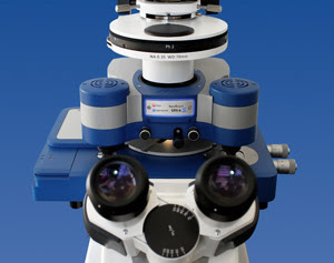
| JPK's new NanoWizard® ULTRA Speed AFM mounted on a Zeiss Axiovert microscope |
Abstract:
JPK Instruments, a world-leading manufacturer of nanoanalytic instrumentation for research in life sciences and soft matter, announces the release of the next generation of NanoWizard® AFM systems delivering fast-scanning and super-resolution on an inverted microscope.
JPK launches the fast-scanning & super-resolution NanoWizard ULTRA Speed AFM system
Berlin, Germany | Posted on December 12th, 2013The boundaries for performance of analytical instrumentation are continually being pushed to the limits. In the world of atomic force microscopy, AFM, JPK Instruments have launched a new AFM system capable of delivering fast-scanning and super-resolution on a single instrument platform, the NanoWizard® ULTRA Speed AFM. The fast scanning NanoWizard® ULTRA Speed AFM is important to users as it enables the tracking of changes in samples in real time whether the sample be imaged in air or liquid. Scanning at speeds of greater than 100Hz line rate with excellent, true atomic resolution in closed-loop mode is enabled by the enhanced low noise of scanner, position sensor and detection system. The new AFM system uses JPK's unique QI™ (Quantitative Imaging) mode to provide quantitative material property mapping.
As with previous NanoWizard® systems, the ULTRA Speed AFM may be fully integrated with an inverted optical microscope thanks to its tip-scanning design and DirectOverlay™ mode for the most precise correlative microscopy. Similarly, the system provides extensive force measurement capability making measurements on single molecules or on living cells thanks to the JPK RampDesigner™ and ExperimentPlanner™. The system is fully compatible with JPK's unsurpassed range of imaging modes and accessories especially for environmental control of the sample.
Speaking about the announcement of the NanoWizard® ULTRA Speed AFM, founder and Chief Technical Officer, Torsten Jähnke, says that "Once again JPK have set a new standard in terms of resolution paired with scan speed. We have managed to develop the lowest noise cantilever deflection system which, when put with our latest fast, high bandwidth electronics, is able to deliver the most accurate force control system even on the most delicate of samples, perfect for users studying biological or other soft matter systems. It is the best multipurpose, fast and high-resolution machine on an inverted microscope today."
For more details about JPK's NanoWizard® ULTRA Speed AFM and applications for the bio & nano sciences, please contact JPK on +49 30533112070, visit the web site: http://www.jpk.com/ or see more on Facebook: www.jpk.com/facebook and on You Tube: www.youtube.com/jpkinstruments.
####
About JPK Instruments
JPK Instruments AG is a world-leading manufacturer of nanoanalytic instruments - particularly atomic force microscope (AFM) systems and optical tweezers - for a broad range of applications reaching from soft matter physics to nano-optics, from surface chemistry to cell and molecular biology. From its earliest days applying atomic force microscope (AFM) technology, JPK has recognized the opportunities provided by nanotechnology for transforming life sciences and soft matter research. This focus has driven JPK's success in uniting the worlds of nanotechnology tools and life science applications by offering cutting-edge technology and unique applications expertise. Headquartered in Berlin and with direct operations in Dresden, Cambridge (UK), Singapore, Tokyo and Paris (France), JPK maintains a global network of distributors and support centers and provides on the spot applications and service support to an ever-growing community of researchers.
For more information, please click here
Contacts:
JPK Instruments AG
Bouchéstrasse 12
Haus 2, Aufgang C
Berlin 12435
Germany
T +49 30533112070
F +49 30 5331 22555
http://www.jpk.com/
Talking Science Limited
39 de Bohun Court
Saffron Walden
Essex CB10 2BA
United Kingdom
T +44(0)1799 521881
M +44(0)7843 012997
http://www.talking-science.com/
Issuers of news releases, not 7th Wave, Inc. or Nanotechnology Now, are solely responsible for the accuracy of the content.
| Related News Press |
News and information
![]() Quantum computer improves AI predictions April 17th, 2026
Quantum computer improves AI predictions April 17th, 2026
![]() Flexible sensor gains sensitivity under pressure April 17th, 2026
Flexible sensor gains sensitivity under pressure April 17th, 2026
![]() A reusable chip for particulate matter sensing April 17th, 2026
A reusable chip for particulate matter sensing April 17th, 2026
![]() Detecting vibrational quantum beating in the predissociation dynamics of SF6 using time-resolved photoelectron spectroscopy April 17th, 2026
Detecting vibrational quantum beating in the predissociation dynamics of SF6 using time-resolved photoelectron spectroscopy April 17th, 2026
Imaging
![]() Simple algorithm paired with standard imaging tool could predict failure in lithium metal batteries August 8th, 2025
Simple algorithm paired with standard imaging tool could predict failure in lithium metal batteries August 8th, 2025
Announcements
![]() A fundamentally new therapeutic approach to cystic fibrosis: Nanobody repairs cellular defect April 17th, 2026
A fundamentally new therapeutic approach to cystic fibrosis: Nanobody repairs cellular defect April 17th, 2026
![]() UC Irvine physicists discover method to reverse ‘quantum scrambling’ : The work addresses the problem of information loss in quantum computing system April 17th, 2026
UC Irvine physicists discover method to reverse ‘quantum scrambling’ : The work addresses the problem of information loss in quantum computing system April 17th, 2026
Tools
![]() Metasurfaces smooth light to boost magnetic sensing precision January 30th, 2026
Metasurfaces smooth light to boost magnetic sensing precision January 30th, 2026
![]() From sensors to smart systems: the rise of AI-driven photonic noses January 30th, 2026
From sensors to smart systems: the rise of AI-driven photonic noses January 30th, 2026
![]() Japan launches fully domestically produced quantum computer: Expo visitors to experience quantum computing firsthand August 8th, 2025
Japan launches fully domestically produced quantum computer: Expo visitors to experience quantum computing firsthand August 8th, 2025
|
|
||
|
|
||
| The latest news from around the world, FREE | ||
|
|
||
|
|
||
| Premium Products | ||
|
|
||
|
Only the news you want to read!
Learn More |
||
|
|
||
|
Full-service, expert consulting
Learn More |
||
|
|
||


