Home > Press > Taking a New Look at Carbon Nanotubes: Berkeley Researchers Develop Technique For Imaging Individual Carbon Nanotubes
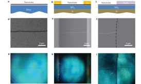 |
| In this display showing optical imaging and spectroscopy of an individual nanotube on substrates and in devices, (a�c) are schematics of a nanotube on a fused-silica substrate, in a field-effect transistor device with two gold electrodes, and under an alumina dielectric layer; (d�f) are SEM images and (g-i) are direct optical images of these individual nanotubes. |
Abstract:
Despite their almost incomprehensibly small size - a diameter about one ten-thousandth the thickness of a human hair - single-walled carbon nanotubes come in a plethora of different "species," each with its own structure and unique combination of electronic and optical properties. Characterizing the structure and properties of an individual carbon nanotube has involved a lot of guesswork - until now.
Taking a New Look at Carbon Nanotubes: Berkeley Researchers Develop Technique For Imaging Individual Carbon Nanotubes
Berkeley, CA | Posted on November 12th, 2013Researchers with the U.S. Department of Energy (DOE)'s Lawrence Berkeley National Laboratory (Berkeley Lab) and the University of California (UC) Berkeley have developed a technique that can be used to identify the structure of an individual carbon nanotube and characterize its electronic and optical properties in a functional device.
"Using a novel high-contrast polarization-based optical microscopy set-up, we've demonstrated video-rate imaging and in-situ spectroscopy of individual carbon nanotubes on various substrates and in functional devices," says Feng Wang, a condensed matter physicist with Berkeley Lab's Materials Sciences Division. "For the first time, we can take images and spectra of individual nanotubes in a general environment, including on substrates or in functional devices, which should be a great tool for advancing nanotube technology."
Wang, who is also a professor with UC Berkeley's Physics Department, is the corresponding author of a paper describing this research in the journal Nature Nanotechnology. The paper is titled "High-throughput optical imaging and spectroscopy of individual carbon nanotubes in devices." Co-authors are Kaihui Liu, Xiaoping Hong, Qin Zhou, Chenhao Jin, Jinghua Li, Weiwei Zhou, Jie Liu, Enge Wang and Alex Zettl.
A single-walled carbon nanotube can be metallic or semiconducting depending on its exact structure. Semiconducting nanotubes can have very different electronic bandgaps, resulting in wildly different electronic or optical properties.
"To fully understand field-effect devices or optoelectronic devices made from single-walled carbon nanotubes, it is critical to know what species of carbon nanotube is in the device," Wang says. "In the past, such information could not be obtained and researchers had to guess as to what was going on."
The physical structure and electronic properties of each individual species of single-walled carbon nanotubes are governed by chirality, meaning their structure has a distinct left/right orientation or "handedness," which cannot be superimposed on a mirror image. As a result, achieving chirality-controlled growth of carbon nanotubes and understanding the physics behind chirality-dependent devices are two of the biggest challenges in nanotube research.
"Polarization-based optical microscopy and spectroscopy techniques are well-suited for meeting these challenges, as polarized light is extremely sensitive to optical anisotropy in a system and has long been exploited to study chirality in molecules and crystals," Wang says. "However, the small signal and unavoidable environment background has made it difficult to use polarized optical microscopy to study single carbon nanotubes."
Difficulties arise from an apparent contradiction in polarization-based optical microscopy. For any optical microscope, a large numerical aperture (NA) objective is crucial for high-spatial resolution, but polarized light passing through a large NA objective becomes strongly depolarized. With their new technique, Wang and his colleagues were able to do what has not been done before and simultaneously achieve both high polarization and high spatial resolution.
"The key to our success was the realization that light illumination and light collection can be controlled separately," Wang says. "We used a large NA objective for light collection to obtain high spatial resolution, but were able to create an effectively small NA objective for illumination to maintain high polarization purity."
In their set-up, Wang and his colleagues collected nanotube-scattered polarized light with a 0.8 NA objective but used a much more narrow incident beam to create illumination light from a supercontinuum laser with a much smaller NA. The result was polarization an order of magnitude higher than what has been achieved with conventional polarized microscopy and spatial resolution at the nanoscale. This enabled them to obtain complete chirality profiles of hundreds of as-grown carbon nanotubes, and to perform in-situ monitoring in active field-effect devices.
"We observed that high order nanotube optical resonances are dramatically broadened by electrostatic doping, an unexpected behavior that points to strong inter-band electron-electron scattering processes dominating the ultrafast dynamics of excited states in carbon nanotubes," Wang says.
In addition to individual single-walled carbon nanotubes, Wang and his colleagues say their technique can also be used to greatly enhance the optical contrast of other anisotropic nano-sized materials that are "invisible" to conventional optical microscopes, including graphene nanoribbons, semiconductor nanowires and nanorods, and nanobiomaterials such as actin filaments.
This research was supported by grants from the National Science Foundation, the Center for Integrated Nanomechanical Systems, and by DOE's Office of Science.
####
About Berkeley Lab
Lawrence Berkeley National Laboratory (Berkeley Lab) addresses the world�s most urgent scientific challenges by advancing sustainable energy, protecting human health, creating new materials, and revealing the origin and fate of the universe. Founded in 1931, Berkeley Lab�s scientific expertise has been recognized with 13 Nobel prizes. The University of California manages Berkeley Lab for the U.S. Department of Energy�s Office of Science. For more, visit www.lbl.gov.
DOE�s Office of Science is the single largest supporter of basic research in the physical sciences in the United States, and is working to address some of the most pressing challenges of our time. For more information, please visit the Office of Science website at science.energy.gov.
For more information, please click here
Contacts:
Lynn Yarris
510-486-5375
Copyright © Berkeley Lab
If you have a comment, please Contact us.Issuers of news releases, not 7th Wave, Inc. or Nanotechnology Now, are solely responsible for the accuracy of the content.
Bookmark:


| Related Links |
![]() For more about the research of Feng Wang go here:
For more about the research of Feng Wang go here:
| Related News Press |
News and information
![]() Quantum computer improves AI predictions April 17th, 2026
Quantum computer improves AI predictions April 17th, 2026
![]() Flexible sensor gains sensitivity under pressure April 17th, 2026
Flexible sensor gains sensitivity under pressure April 17th, 2026
![]() A reusable chip for particulate matter sensing April 17th, 2026
A reusable chip for particulate matter sensing April 17th, 2026
![]() Detecting vibrational quantum beating in the predissociation dynamics of SF6 using time-resolved photoelectron spectroscopy April 17th, 2026
Detecting vibrational quantum beating in the predissociation dynamics of SF6 using time-resolved photoelectron spectroscopy April 17th, 2026
Imaging
![]() Simple algorithm paired with standard imaging tool could predict failure in lithium metal batteries August 8th, 2025
Simple algorithm paired with standard imaging tool could predict failure in lithium metal batteries August 8th, 2025
![]() First real-time observation of two-dimensional melting process: Researchers at Mainz University unveil new insights into magnetic vortex structures August 8th, 2025
First real-time observation of two-dimensional melting process: Researchers at Mainz University unveil new insights into magnetic vortex structures August 8th, 2025
![]() New imaging approach transforms study of bacterial biofilms August 8th, 2025
New imaging approach transforms study of bacterial biofilms August 8th, 2025
Laboratories
![]() Researchers develop molecular qubits that communicate at telecom frequencies October 3rd, 2025
Researchers develop molecular qubits that communicate at telecom frequencies October 3rd, 2025
Govt.-Legislation/Regulation/Funding/Policy
![]() Quantum computer improves AI predictions April 17th, 2026
Quantum computer improves AI predictions April 17th, 2026
![]() Metasurfaces smooth light to boost magnetic sensing precision January 30th, 2026
Metasurfaces smooth light to boost magnetic sensing precision January 30th, 2026
![]() New imaging approach transforms study of bacterial biofilms August 8th, 2025
New imaging approach transforms study of bacterial biofilms August 8th, 2025
Nanotubes/Buckyballs/Fullerenes/Nanorods/Nanostrings/Nanosheets
![]() Tiny nanosheets, big leap: A new sensor detects ethanol at ultra-low levels January 30th, 2026
Tiny nanosheets, big leap: A new sensor detects ethanol at ultra-low levels January 30th, 2026
![]() Enhancing power factor of p- and n-type single-walled carbon nanotubes April 25th, 2025
Enhancing power factor of p- and n-type single-walled carbon nanotubes April 25th, 2025
![]() Chainmail-like material could be the future of armor: First 2D mechanically interlocked polymer exhibits exceptional flexibility and strength January 17th, 2025
Chainmail-like material could be the future of armor: First 2D mechanically interlocked polymer exhibits exceptional flexibility and strength January 17th, 2025
![]() Innovative biomimetic superhydrophobic coating combines repair and buffering properties for superior anti-erosion December 13th, 2024
Innovative biomimetic superhydrophobic coating combines repair and buffering properties for superior anti-erosion December 13th, 2024
Discoveries
![]() Quantum computer improves AI predictions April 17th, 2026
Quantum computer improves AI predictions April 17th, 2026
![]() Flexible sensor gains sensitivity under pressure April 17th, 2026
Flexible sensor gains sensitivity under pressure April 17th, 2026
![]() A reusable chip for particulate matter sensing April 17th, 2026
A reusable chip for particulate matter sensing April 17th, 2026
![]() Detecting vibrational quantum beating in the predissociation dynamics of SF6 using time-resolved photoelectron spectroscopy April 17th, 2026
Detecting vibrational quantum beating in the predissociation dynamics of SF6 using time-resolved photoelectron spectroscopy April 17th, 2026
Announcements
![]() A fundamentally new therapeutic approach to cystic fibrosis: Nanobody repairs cellular defect April 17th, 2026
A fundamentally new therapeutic approach to cystic fibrosis: Nanobody repairs cellular defect April 17th, 2026
![]() UC Irvine physicists discover method to reverse �quantum scrambling� : The work addresses the problem of information loss in quantum computing system April 17th, 2026
UC Irvine physicists discover method to reverse �quantum scrambling� : The work addresses the problem of information loss in quantum computing system April 17th, 2026
Interviews/Book Reviews/Essays/Reports/Podcasts/Journals/White papers/Posters
![]() A fundamentally new therapeutic approach to cystic fibrosis: Nanobody repairs cellular defect April 17th, 2026
A fundamentally new therapeutic approach to cystic fibrosis: Nanobody repairs cellular defect April 17th, 2026
![]() UC Irvine physicists discover method to reverse �quantum scrambling� : The work addresses the problem of information loss in quantum computing system April 17th, 2026
UC Irvine physicists discover method to reverse �quantum scrambling� : The work addresses the problem of information loss in quantum computing system April 17th, 2026
Tools
![]() Metasurfaces smooth light to boost magnetic sensing precision January 30th, 2026
Metasurfaces smooth light to boost magnetic sensing precision January 30th, 2026
![]() From sensors to smart systems: the rise of AI-driven photonic noses January 30th, 2026
From sensors to smart systems: the rise of AI-driven photonic noses January 30th, 2026
![]() Japan launches fully domestically produced quantum computer: Expo visitors to experience quantum computing firsthand August 8th, 2025
Japan launches fully domestically produced quantum computer: Expo visitors to experience quantum computing firsthand August 8th, 2025
|
|
||
|
|
||
| The latest news from around the world, FREE | ||
|
|
||
|
|
||
| Premium Products | ||
|
|
||
|
Only the news you want to read!
Learn More |
||
|
|
||
|
Full-service, expert consulting
Learn More |
||
|
|
||