Home > Press > Perfect faults: A self-correcting crystal may unleash the next generation of advanced communications
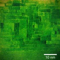 |
| Not a brick wall. Electron microscope image of a cross section of the newly characterized tunable microwave dielectric clearly shows the thick layers of strontium titanate "bricks" separated by thin "mortar lines" of strontium oxide that help promote the largely defect-free growth of the bricks.
Credit: TEM image courtesy David Mueller. Color added for clarity by Nathan Orloff. |
Abstract:
Researchers from the National Institute of Standards and Technology (NIST) have joined with an international team to engineer and measure a potentially important new class of nanostructured materials for microwave and advanced communication devices. Based on NIST's measurements, the new materials—a family of multilayered crystalline sandwiches—might enable a whole new class of compact, high-performance, high-efficiency components for devices such as cellular phones.*
Perfect faults: A self-correcting crystal may unleash the next generation of advanced communications
Gaithersburg, MD | Posted on November 6th, 2013"These materials are an excellent example of what the Materials Genome Initiative refers to as 'materials-by-design'," says NIST physicist James Booth, one of the lead researchers. "Materials science is getting better and better at engineering complex structures at an atomic scale to create materials with previously unheard-of properties."
The new multilayer crystals are so-called "tunable dielectrics," the heart of electronic devices that, for example, enable cell phones to tune to a precise frequency, picking a unique signal out of the welter of possible ones.
Tunable dielectrics that work well in the microwave range and beyond—modern communications applications typically use frequencies around a few gigahertz—have been hard to make, according to NIST materials scientist Nathan Orloff. "People have created tunable microwave dielectrics for decades, but they've always used up way too much power." These new materials work well up to 100 GHz, opening the door for the next generation of devices for advanced communications.
Modern cellphone dielectrics use materials that suffer from misplaced or missing atoms called "defects" within their crystal structure, which interfere with the dielectric properties and lead to power loss. One major feature of the new materials, says Orloff, is that they self-correct, reducing the effect of defects in the part of the crystal where it counts. "We refer to this material as having 'perfect faults'," he says. "When it's being grown, one portion accommodates defects without affecting the good parts of the crystal. It's able to correct itself and create perfect dielectric bricks that result in the rare combination of high tuning and low loss."
The new material has layers of strontium oxide, believed to be responsible for the self-correcting feature, separating a variable number of layers of strontium titanate. Strontium titanate on its own is normally a pretty stable dielectric—not really tunable at all—but another bit of nanostructure wizardry solves that. The sandwich layers are grown as a thin crystalline film on top of a substrate material with a mismatched crystal spacing that produces strain within the strontium titanate structure that makes it a less stable dielectric—but one that can be tuned. "It's like putting a queen-sized sheet on a king-sized bed," says Orloff. "The combination of strain with defect control leads to the unique electronic properties."
One key discovery by the research team was that, in addition to adding strain to the crystal sandwich, adding additional layers of strontium titanate in between the strontium oxide layers increased the room-temperature "tunability" performance of the structure, providing a new mechanism to control the material response. The material they reported on recently in the journal Nature has six layers of strontium titanate between each strontium oxide layer.
The new sandwich material performs so well as a tunable dielectric, over such a broad range of frequencies, that the NIST team led by Booth had to develop a new measurement technique—an array of test structures fabricated on top of the test film—just to measure its electronic characteristics. "We were able to characterize the performance of these materials as a function of frequency running from 10 hertz all the way up to 125 gigahertz. That's the equivalent of measuring wavelengths from kilometers down to microns all with the same experimental set-up," says Orloff, adding, "This material has a much lower loss and a much higher tunability for a given applied field then any material that we have seen."
An international team of researchers contributed to the recent paper, representing, in addition to NIST, Cornell University, the University of Maryland, Pennsylvania State University, the Institute of Physics ASCR (Czech Republic), Universitat Politčcnica de Catalunya (Spain), the Kavli Institute at Cornell for Nanoscale Science, Oak Ridge National Laboratory, the Leibniz Institute for Crystal Growth (Germany), The University of Texas at Austin and Temple University.
*C-H Lee, N.D. Orloff, T. Birol, Y. Zhu, V. Goian, E. Rocas, R. Haislmaier, E. Vlahos, J.A. Mundy, L.F. Kourkoutis, Y. Nie, M.D. Biegalski, J. Zhang, M. Bernhagen, N.A. Benedek, Y. Kim, J.D. Brock, R.Uecker, X.X. Xi, V. Gopalan, D. Nuzhnyy, S. Kamba, D.A. Muller, I. Takeuchi, J.C. Booth, C.J. Fennie and D.G. Schlom. Exploiting dimensionality and defect mitigation to create tunable microwave dielectrics. Nature, 502, 532-536, Oct. 24, 2013. doi:10.1038/nature12582.
####
About National Institute of Standards and Technology (NIST)
The National Institute of Standards and Technology (NIST) is an agency of the U.S. Department of Commerce.
For more information, please click here
Contacts:
Michael Baum
301-975-2763
Copyright © National Institute of Standards and Technology (NIST)
If you have a comment, please Contact us.Issuers of news releases, not 7th Wave, Inc. or Nanotechnology Now, are solely responsible for the accuracy of the content.
Bookmark:


| Related Links |
![]() For more on the MGI at NIST, see:
For more on the MGI at NIST, see:
| Related News Press |
News and information
![]() Quantum computer improves AI predictions April 17th, 2026
Quantum computer improves AI predictions April 17th, 2026
![]() Flexible sensor gains sensitivity under pressure April 17th, 2026
Flexible sensor gains sensitivity under pressure April 17th, 2026
![]() A reusable chip for particulate matter sensing April 17th, 2026
A reusable chip for particulate matter sensing April 17th, 2026
![]() Detecting vibrational quantum beating in the predissociation dynamics of SF6 using time-resolved photoelectron spectroscopy April 17th, 2026
Detecting vibrational quantum beating in the predissociation dynamics of SF6 using time-resolved photoelectron spectroscopy April 17th, 2026
Wireless/telecommunications/RF/Antennas/Microwaves
![]() Researchers develop molecular qubits that communicate at telecom frequencies October 3rd, 2025
Researchers develop molecular qubits that communicate at telecom frequencies October 3rd, 2025
![]() HKUST researchers develop new integration technique for efficient coupling of III-V and silicon February 16th, 2024
HKUST researchers develop new integration technique for efficient coupling of III-V and silicon February 16th, 2024
Laboratories
![]() Researchers develop molecular qubits that communicate at telecom frequencies October 3rd, 2025
Researchers develop molecular qubits that communicate at telecom frequencies October 3rd, 2025
Govt.-Legislation/Regulation/Funding/Policy
![]() Quantum computer improves AI predictions April 17th, 2026
Quantum computer improves AI predictions April 17th, 2026
![]() Metasurfaces smooth light to boost magnetic sensing precision January 30th, 2026
Metasurfaces smooth light to boost magnetic sensing precision January 30th, 2026
![]() New imaging approach transforms study of bacterial biofilms August 8th, 2025
New imaging approach transforms study of bacterial biofilms August 8th, 2025
Chip Technology
![]() A reusable chip for particulate matter sensing April 17th, 2026
A reusable chip for particulate matter sensing April 17th, 2026
![]() Metasurfaces smooth light to boost magnetic sensing precision January 30th, 2026
Metasurfaces smooth light to boost magnetic sensing precision January 30th, 2026
Discoveries
![]() Quantum computer improves AI predictions April 17th, 2026
Quantum computer improves AI predictions April 17th, 2026
![]() Flexible sensor gains sensitivity under pressure April 17th, 2026
Flexible sensor gains sensitivity under pressure April 17th, 2026
![]() A reusable chip for particulate matter sensing April 17th, 2026
A reusable chip for particulate matter sensing April 17th, 2026
![]() Detecting vibrational quantum beating in the predissociation dynamics of SF6 using time-resolved photoelectron spectroscopy April 17th, 2026
Detecting vibrational quantum beating in the predissociation dynamics of SF6 using time-resolved photoelectron spectroscopy April 17th, 2026
Announcements
![]() A fundamentally new therapeutic approach to cystic fibrosis: Nanobody repairs cellular defect April 17th, 2026
A fundamentally new therapeutic approach to cystic fibrosis: Nanobody repairs cellular defect April 17th, 2026
![]() UC Irvine physicists discover method to reverse ‘quantum scrambling’ : The work addresses the problem of information loss in quantum computing system April 17th, 2026
UC Irvine physicists discover method to reverse ‘quantum scrambling’ : The work addresses the problem of information loss in quantum computing system April 17th, 2026
Interviews/Book Reviews/Essays/Reports/Podcasts/Journals/White papers/Posters
![]() A fundamentally new therapeutic approach to cystic fibrosis: Nanobody repairs cellular defect April 17th, 2026
A fundamentally new therapeutic approach to cystic fibrosis: Nanobody repairs cellular defect April 17th, 2026
![]() UC Irvine physicists discover method to reverse ‘quantum scrambling’ : The work addresses the problem of information loss in quantum computing system April 17th, 2026
UC Irvine physicists discover method to reverse ‘quantum scrambling’ : The work addresses the problem of information loss in quantum computing system April 17th, 2026
Research partnerships
![]() Lab to industry: InSe wafer-scale breakthrough for future electronics August 8th, 2025
Lab to industry: InSe wafer-scale breakthrough for future electronics August 8th, 2025
![]() HKU physicists uncover hidden order in the quantum world through deconfined quantum critical points April 25th, 2025
HKU physicists uncover hidden order in the quantum world through deconfined quantum critical points April 25th, 2025
|
|
||
|
|
||
| The latest news from around the world, FREE | ||
|
|
||
|
|
||
| Premium Products | ||
|
|
||
|
Only the news you want to read!
Learn More |
||
|
|
||
|
Full-service, expert consulting
Learn More |
||
|
|
||